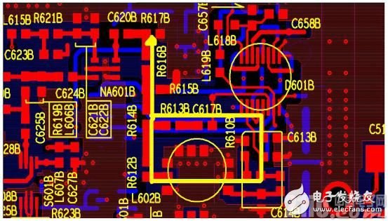
Single-frequency comprehensive layout. Usually take the shape of the figure to be laid out: the left arm branch is the reference frequency source and the PLL control circuit, and the right arm branch is the voltage controlled oscillator (VCO) output isolation amplifier circuit. The central ring is a phase-locked loop (PLL)

Ping-pong switching frequency synthesis layout, also called tuning fork layout: the two arms of the tuning fork are symmetric two PLL frequency synthesis, and the arm intersection is a switching device. The common arm is a two-way output amplifier after switching.
Multi-channel transceiver transceiver or transmitter local oscillator level distribution circuit layout: symmetrical tree layout.
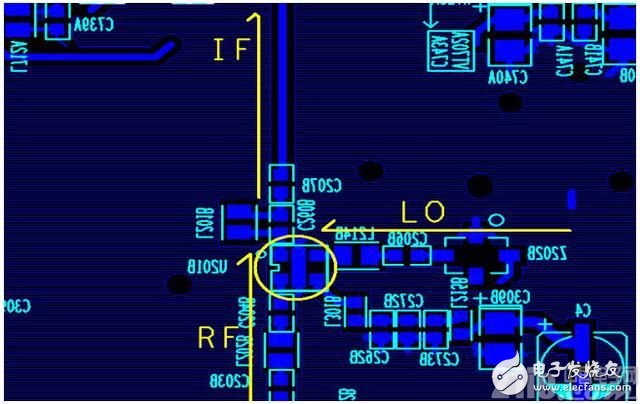
2 Mixer (MIXER) circuit layoutMixing circuit, also known as the up-down frequency conversion circuit, is an important part of the transmitter and super-heterodyne receiver. It is a typical spectrum shift circuit. For receivers, the principle is to downconvert the received RF signal and local oscillator circuit (LO) to generate a lower-frequency IF signal. The IF signal is amplified and then detected to restore original signal. For the transmitter, the principle is to up-convert the intermediate frequency signal and the local oscillator circuit to generate a higher RF signal. The RF signal is amplified and then transmitted.
The T word layout is the same. The following figure shows a typical mixer layout:

The T word layout is different: the up-conversion mode: the RF branch is different from the LO branch, and the IF branch is the same as the LO. This arrangement minimizes leakage of the LO to the RF branch.
The word layout is different: the down conversion mode: the RF branch is the same as the LO branch, and the IF branch is different from the LO.
3 Acoustic filter circuit layoutThe input and output of the SAW filter are preferably placed on both sides of the PCB. When the input and output circuits are actually routed, the length of the transmission line should be reduced as much as possible; conditions permitting, paving the microstrip line (microstrip line and The distance to the ground is greater than equal to 2 times the width of the microstrip line, and ground holes are drilled along the transmission line at the ground plane. Spaces that are not used are paved; reducing discontinuities in microstrip transmission lines, such as abrupt changes, turnings, etc.
If the input and output circuits are on the same mounting surface of the PCB, they are in the same cavity. The microwave absorbing material should be mounted on the surface of the cavity so as to reduce the reflection and increase the loss of the distributed capacitance, so as to finally reduce the mutual coupling of the input and output circuits.
The inductance of the input matching circuit and the inductance of the output matching circuit are placed perpendicular to each other so that the magnetic field directions of the inductors are perpendicular to each other, thereby reducing the coupling.
At least in the bottom layer of the filter, if it can be more effective. However, it is necessary to separate the input and output ground currents as much as possible. Common ground coupling of input and output ground currents is generally reduced by adding a ground tank. This groove preferably penetrates all dielectric layers.
If the SAW filter has a “RETURN†pin, the path to the RETURN pin should be minimized. If there is no RETURN pin, select the “ground†pin closest to the input and output signal pins as the RETURN pin.
The two SAW filters should be placed in separate shielded chambers. It is also possible to place the two SAWs on the front and back sides of the PCB, and to isolate them through the inner PCB layers. However, it is necessary to avoid overlapping both sides of the PCB. Because stacking means ground sharing, common ground current coupling exists. Affects the performance of the SAW.
When the acoustic table is cascaded with the mixer, the mixer and the acoustic table should be placed in separate shielded chambers.
When the SAW is cascaded with the amplifier, the SAW input matching circuit and the input amplifier are placed in a shielding cavity, and the output matching circuit and the output amplifier are placed in another shielding cavity to ensure sufficient isolation. It is also possible to place the input matching circuit of the SAW input circuit, the input amplifier and the input/output matching circuit, and the output amplifier on the front and back sides of the PCB, and isolate them through the inner layer of the PCB. However, it is necessary to avoid overlapping both sides of the front and back, because the overlapping means that the common ground, there is a common ground current coupling, will affect the performance of the SAW.
When the acoustic table is cascaded with other unit circuits, it is also preferable to consider isolation measures or absorption measures.
Anti-Jamming RC Arc Extinguisher
Anti-Jamming RC Arc Extinguisher

Anti-Jamming RC Arc Extinguisher
YANGZHOU POSITIONING TECH CO., LTD. , https://www.yzpst.com