I know that I'm fascinated by all things related to electronics, but from what point of view, today's Field Programmable Gate Arrays (FPGAs) are "stand out from the crowd," and are really great devices. If in this smart age, in this field, you want to have a skill you have not paid attention to FPGA , then the world will abandon you and the times will abandon you. The public author, ALIFPGA , has many years of experience in FPGA development. All articles are summarizing years of learning and work experience.

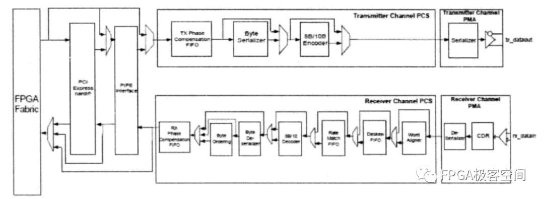
Stratix IV GX embedded SERDES structure as shown
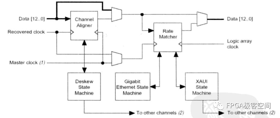
Channel Aligner and Rate Matcher.
Channel Aligner and Rate Matcher align all channels of data according to the PCS (Physical Coding Sub-layer) specification of various interface standards and adapt the data rate to synchronize the state machine. The commonly used interface standards are GE, 10GE and XAUI.

8B/10B decoding.
The 8B/10B decoder performs the 8B/10B decoding function here and converts 10 bit data to 8 bit source data.
Receive end to logical resource interface.
The data recovered from the SERDES enters the FPGA with a problem of demultiplexing and clock domain conversion. The Stratix GX contains dedicated circuits capable of performing 8/10-bit data to 8/10/20-bit Mux/Demux, and the SERDES receiver to the FPGA. There are FIFOs between general logic resources to complete data interface synchronization. The circuit structure is shown in the figure.

The structure of the sending direction is relatively simple. It is easy to understand the function and structure of the originating main module as long as the data is traced backward according to the direction of the end data. The originator mainly includes the following functional modules.
(1) FPGA logic data SERDES originating interface circuit.
From FPGA logic resources to the end of the embedded 8-byte deep FIFO to complete the data interface synchronization, in addition to Mux / Demux circuit, and its structure and end of the FPGA logic resource interface circuit.
(2) 8B/10B encoding.
Encode 8bit source data into 10bit data and reduce "0" or even "1" strings.
(3) Originating PLL.
The originating PLL parameters are shown in the figure.
(4) Serializer circuit (Serializer).
The parallel-to-serial conversion sequence is a low-order (LSB) first-out.
(5) Output buffer.
Its supported I/O standards and programmable matching impedance characteristics are similar to the end-of-end buffering performance. It is worth mentioning that the dynamic programmable range of its Vod voltage is 400Mv~1600mV, and the new device's pre-emphasis range is increased from 0% to 140% (Vod is 800mV).
It is worth emphasizing that the SERDES module of Altera's Stratix GX is very testable, providing a rich loopback mode that is easy for users to debug on the board. Stratix GX's SERDES supports the following test modes.
Channel loopback: includes serial loopback, reverse serial loopback, parallel loopback, and direction link parallel loopback. Parallel loopback) 4 modes.
BIST (Built-In Self Test) BIST generator & verifier: Includes BIST 8B parallel loopback, BIST parallel loopback, and BIST serial loopback.
BIST generator & verifier: Includes PRBS parallel loopback and PRBS serial loopback
Cell Phone Case, Mobile Phone Covers, Clear Phone Case, Mobile Phone Case, TPU Phone Case, Silicone Phone Case
Shenzhen Jianjiantong Technology Co., Ltd. , https://www.jjtphonesticker.com