Abstract: The MAX1455 high-performance low-cost signal condiTIoner includes output clipping capability, which is very important diagnosTIc tool in the automoTIve applicaTIons. This feature can detect various failure mode of the transducer module, including the failed sensors. When a resistive load is applied to the OUT pin during clip, the clip voltage is pulled away from the nominal set point. A solution is presented that prevents output loading from changing the clip voltage value. This is accomplished by using the on-chip uncommitted op amp as a buffer . The PGA and clip circuit output the full voltage range from clip-low to clip-high and the op amp drives the resistive load. This document also describes a way of customizing the pre-programmed clipping limits.
The MAX1455 has a unique feature: programmable analog clip-levels on the output signal. This feature can detect open circuits and short circuits in the wiring harness and connectors. It can also detect failed sensors.
The output clip functions, Clip-Top and Clip-Bot, set the upper and lower output voltage limits of the programmable gain amplifier (PGA). The clip functions are highlighted in the MAX1455 block diagram in Figure 1.
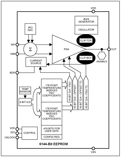
Figure 1. Block diagram shows the diagnostic functions clip-top and clip-bot at the PGA output.
A typical application diagram is shown in Figure 2. The sensor assembly contains a pressure or force transducer and the MAX1455 signal conditioning IC. A wiring harness joins the sensor assembly to the primary Electronic Control Unit (ECU). The ECU provides the power-supply voltage (5V typical) to the sensor and receives the analog voltage signal from the sensor. The three harness wires are often bundled with other wires and may pass through several connector systems between the sensor and the ECU. It is desirable to detect an open circuit in the wires or connectors so that the ECU can take appropriate action. This action may consist of shutting down a subsystem, disregarding all measurements on the suspect line, or activating warning lights to indicate the fault condition.
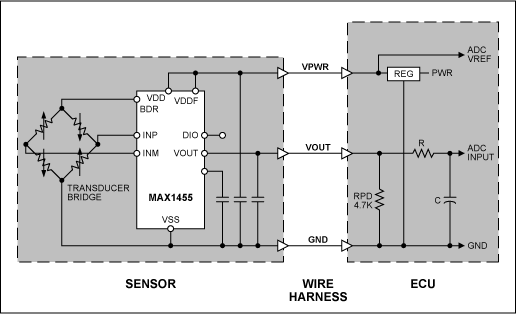
Figure 2. Typical sensor wiring configuration.
It has become common practice to use a pull-up or pull-down resistor on the Vout line in the ECU that will pull the line to a defined state when the Vout line is an open circuit, as shown in Figure 2. Values ​​for RPU or RPD of 2.2KΩ to 10KΩ have been used. When the Vout line is an open circuit the resistor pulls the line to a supply-rail and keeps it stable at that value. Normally this would be confused with a no-load, or full -scale load condition. By limiting the normal operating output of the sensor to values ​​that are slightly away from the supply-rail voltages, a supply-rail voltage then is defined as an anomaly or fault condition (ie, an open circuit in the Vout line).
When low values ​​of RPU or RPD are used, and precise control of the clip voltage value is desired, it is sometimes necessary to buffer the clipped voltage to prevent the load from pulling the Vout signal away from the programmed clip setting.
The possible clip voltage settings for the MAX1455 are shown in Table 1.
Table 1. Output Clip Voltage Settings with VDD = 5.0VDC
The architecture employed in the MAX1455 to produce the clip levels causes the output impedance to change when transitioning from the active-region (no clipping, valid output) to the clip-region (OUT saturated at clip-high or clip-low). The impedance change is ROUT <2Ω in active-region to ROUT ~ 130Ω during clip. When an output load is applied to the OUT pin during clip, the clip voltage is pulled away from the nominal set point. In a typical application, a 4.7KΩ resistor will be connected to the OUT signal line in the ECU and also connected to Gnd or VSS. This load will pull the clip-high voltage off the set value by 128mV resulting in VCLIPHIGH = 4.622v when set to a clip value of 4.75V .
A solution that prevents output loading from changing the clip voltage value uses the uncommitted op-amp as a buffer as shown in Figure 3. The PGA and clip circuit outputs the full voltage range from clip-low to clip-high and the op-amp drives the resistor load. The op-amp is capable of driving the load to either rail, but limits with the input signal clip levels.
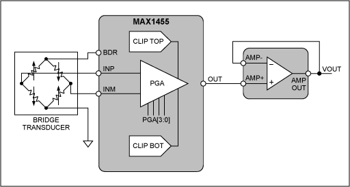
Figure 3. Utilizing the uncommitted op-amp as an output driver / buffer.
The impedance of the output during clip can even be leveraged to produce new clip voltage levels that are also insensitive to output loading effects. For example, a target specification for VCLIP-HIGH = 4.70V can be met by making a minor circuit change as shown in Figure 4. The principle change is to add a resistor RADJ on the MAX1455 OUT line to intentionally pull the clip voltage off the set value and to a new, desired value. The auxiliary op-amp is again used as the primary output signal driver operating as a unity gain buffer.
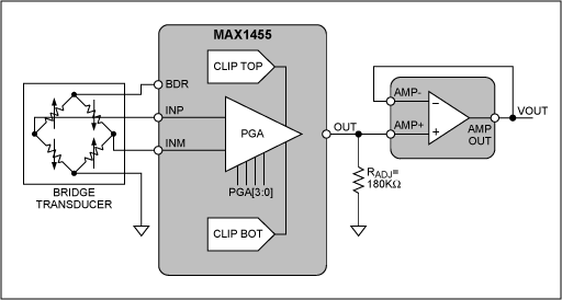
Figure 4. Intentionally pulling the clip voltage off set value and to a new desired value with RADJ.
The clip set points used are CLIP [1: 0] = 11, corresponding to clip-high. Clip-low = 4.75 / 2.50V. The clip-high set point voltage has an intrinsic offset of ?? E0mV due to internal fixed circuit configuration. The resistor RADJ has no influence on the OUT signal when OUT is in the active-region (0.250V <VOUT <4.750V), due to ROUT being <2Ω. However, the clip-high voltage will be reduced, due to the load of RADJ, and produce an actual output clip level of 4.70V.
VCLIP-HIGH (actual) = 4.75V ?? E21mV ?? E130Ω x (4.75V-0.21V) / (130Ω + 18kΩ) = 4.70V
Other clip voltages values ​​can be obtained in a similar manner.
The MAX1455 has a unique feature: programmable analog clip-levels on the output signal. This feature can detect open circuits and short circuits in the wiring harness and connectors. It can also detect failed sensors.
The output clip functions, Clip-Top and Clip-Bot, set the upper and lower output voltage limits of the programmable gain amplifier (PGA). The clip functions are highlighted in the MAX1455 block diagram in Figure 1.

Figure 1. Block diagram shows the diagnostic functions clip-top and clip-bot at the PGA output.
A typical application diagram is shown in Figure 2. The sensor assembly contains a pressure or force transducer and the MAX1455 signal conditioning IC. A wiring harness joins the sensor assembly to the primary Electronic Control Unit (ECU). The ECU provides the power-supply voltage (5V typical) to the sensor and receives the analog voltage signal from the sensor. The three harness wires are often bundled with other wires and may pass through several connector systems between the sensor and the ECU. It is desirable to detect an open circuit in the wires or connectors so that the ECU can take appropriate action. This action may consist of shutting down a subsystem, disregarding all measurements on the suspect line, or activating warning lights to indicate the fault condition.

Figure 2. Typical sensor wiring configuration.
It has become common practice to use a pull-up or pull-down resistor on the Vout line in the ECU that will pull the line to a defined state when the Vout line is an open circuit, as shown in Figure 2. Values ​​for RPU or RPD of 2.2KΩ to 10KΩ have been used. When the Vout line is an open circuit the resistor pulls the line to a supply-rail and keeps it stable at that value. Normally this would be confused with a no-load, or full -scale load condition. By limiting the normal operating output of the sensor to values ​​that are slightly away from the supply-rail voltages, a supply-rail voltage then is defined as an anomaly or fault condition (ie, an open circuit in the Vout line).
When low values ​​of RPU or RPD are used, and precise control of the clip voltage value is desired, it is sometimes necessary to buffer the clipped voltage to prevent the load from pulling the Vout signal away from the programmed clip setting.
The possible clip voltage settings for the MAX1455 are shown in Table 1.
Table 1. Output Clip Voltage Settings with VDD = 5.0VDC
CLIP [1: 0] | Output Clip High (V) | Output Clip Low (V) |
00 | 4.90 | 0.10 |
01 | 4.85 | 0.15 |
10 | 4.80 | 0.20 |
11 | 4.75 | 0.25 |
The architecture employed in the MAX1455 to produce the clip levels causes the output impedance to change when transitioning from the active-region (no clipping, valid output) to the clip-region (OUT saturated at clip-high or clip-low). The impedance change is ROUT <2Ω in active-region to ROUT ~ 130Ω during clip. When an output load is applied to the OUT pin during clip, the clip voltage is pulled away from the nominal set point. In a typical application, a 4.7KΩ resistor will be connected to the OUT signal line in the ECU and also connected to Gnd or VSS. This load will pull the clip-high voltage off the set value by 128mV resulting in VCLIPHIGH = 4.622v when set to a clip value of 4.75V .
A solution that prevents output loading from changing the clip voltage value uses the uncommitted op-amp as a buffer as shown in Figure 3. The PGA and clip circuit outputs the full voltage range from clip-low to clip-high and the op-amp drives the resistor load. The op-amp is capable of driving the load to either rail, but limits with the input signal clip levels.

Figure 3. Utilizing the uncommitted op-amp as an output driver / buffer.
The impedance of the output during clip can even be leveraged to produce new clip voltage levels that are also insensitive to output loading effects. For example, a target specification for VCLIP-HIGH = 4.70V can be met by making a minor circuit change as shown in Figure 4. The principle change is to add a resistor RADJ on the MAX1455 OUT line to intentionally pull the clip voltage off the set value and to a new, desired value. The auxiliary op-amp is again used as the primary output signal driver operating as a unity gain buffer.

Figure 4. Intentionally pulling the clip voltage off set value and to a new desired value with RADJ.
The clip set points used are CLIP [1: 0] = 11, corresponding to clip-high. Clip-low = 4.75 / 2.50V. The clip-high set point voltage has an intrinsic offset of ?? E0mV due to internal fixed circuit configuration. The resistor RADJ has no influence on the OUT signal when OUT is in the active-region (0.250V <VOUT <4.750V), due to ROUT being <2Ω. However, the clip-high voltage will be reduced, due to the load of RADJ, and produce an actual output clip level of 4.70V.
VCLIP-HIGH (actual) = 4.75V ?? E21mV ?? E130Ω x (4.75V-0.21V) / (130Ω + 18kΩ) = 4.70V
Other clip voltages values ​​can be obtained in a similar manner.
Ningbo Autrends International Trade Co.,Ltd. , https://www.vapee-cigarettes.com