With the continuous improvement of LED light efficiency in recent years, the life and reliability of LEDs have received more and more attention from the industry, and it is one of the most important performances of LED products. Every component and link in the manufacture of LED products has an impact on its reliability and longevity. The reliability of solder joints between LED devices and printed circuit boards (PCBs) is critical to ensure the overall reliability of LED luminaires.
This article describes how to use thermal shock testing to analyze the solder joint reliability of Cree XLamp ® high-power LED devices. It is designed to help Cree users master the application and design considerations of Cree LED devices and improve product development efficiency and quality. .
First, the factors affecting the reliability of solder joints
In the LED application design, several solder joints are very important. As shown in Figure 1, the reliability of the three solder joints is the key to ensuring heat transfer from the LED junction to the heat sink.
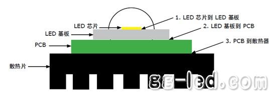
Figure 1 Important solder joints that ensure heat transfer from the LED junction to the heat sink
1. Solder joint of LED chip to LED substrate
This is usually ensured by the LED manufacturer to be complete and reliable, and the following factors should be considered when designing the LED package. 1. Physical properties of LED chips and LED substrates 2. Material selection 3. Solder joint geometry (pad size and shape, placement of pads relative to solder mask) 4. Mechanical properties of bulk solder alloys 5. The nature and structure of the intermetallic compound formed by the point/heat sink interface;
2. LED substrate to PCB solder joints and PCB to heat sink solder joints
The luminaire manufacturer ensures the reliability and integrity of the two solder joints in the application and design. The integrity of the solder joint between the LED substrate and the PCB is one of the main determinants of long-term lumen maintenance and reliability of LED products. Solder joint reliability depends not only on the solder alloy, but also on the metal coating of the LED device and PCB. In addition, the reflow profile has a significant impact on the performance of lead-free solder joints because it affects the wettability and microstructure of the solder joint. Damage or defective solder joints can lead to open circuit failure conditions, which can result in complete failure of the electrical performance of the luminaire.
A key feature to consider when soldering LED devices to PCB reliability is the difference in thermal expansion coefficient between the LED device and the PCB material. Changes in operating conditions can result in different forces due to mismatch in expansion coefficients. These forces may be amplified by some mechanical action (such as bending of the LED substrate). For larger package size LEDs soldered on a rigid PCB, the solder joints furthest away from the center of the LED package have the greatest stress due to expansion mismatch.
In summary, Figure 2 shows the various influencing factors affecting LED solder joints, some of which are highlighted in the text. This study used thermal shock to evaluate the solder joint reliability of selected high power XLamp® LED devices. The rate of temperature rise in the thermal shock test is much higher than in the thermal cycle test, so the damage to the solder joint is much more severe. Through the thermal shock test results, you can gain a deeper understanding of the reliability of solder joints.
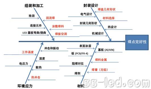
Figure 2 Factors affecting the reliability of LED solder joints
Second, research methods and equipment
In this study, surface mount technology (SMT) reflow soldering process was used to solder LEDs and PCBs, ie LED reels → screen solder paste onto the test board → pick up LED components and place them on the PCB → reflow soldering. Tested with Cree's four high-power XLamp ® LEDs, the dimensions of the different packages are shown in Table 1. The MCPCB board used in this study consists of a solder resist layer, a copper circuit layer, a thin thermally conductive insulating layer, and a metal core substrate layer. These layers are laminated and bonded together to form a heat dissipation path. Each LED has 30 LEDs, and the selected MCPCB board can solder ten LEDs, that is, each LED uses three MCPCB boards.
This study used Indium 8.9 Air Reflow No-Clean Solder Paste, which was formulated to accommodate the high temperatures of tin-silver-copper (SAC) lead-free alloy systems. The solder paste composition includes 96.5% tin (Sn), 3.0% silver (Ag), and 0.5% copper (Cu), which are Class 3 metal loads. The formation of reliable solder joints depends on the time and temperature profile of the reflow process, as well as the ability of the molten solder to wet the surface coating quickly and uniformly, and to form a uniform thickness intermetallic layer at the joint interface by interaction. All of these factors directly affect solder joint formation and reliability. Cree recommends a solder joint thickness of approximately 3 mil (75 μm) after reflow soldering. The solder joint thickness can be verified using an optical microscope with a dial.
The equipment used was an MPM Momentum stencil printer for solder paste printing with a thickness of 6 mils and a template frame size of 73.7 cm x 73.7 cm. Using the JUKI FX-3 placement machine, the Heller 1809 MK III convection reflow oven was used during the reflow process. The reflow oven has eight heating zones and one cooling zone. The reflow soldering process parameters are shown in Table 2. The XLamp ® LEDs used in this study are compatible. JEDEC J-STD-020C standard. More detailed information on Cree XLamp ® LED patch pick and place operations, soldering and handling, and thermal management is available in the application notes provided on the Cree website.
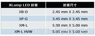
Table 1 Dimensions of selected LED packages

Table 2 Recommended reflow process parameters
Three results analysis
Solder joint cavity
After reflow soldering, the solder joints were visually inspected and no solder joint defects were observed: solder joints, solder bumps, solder bridges, or component rises. In addition, real-time X-ray imaging is used to inspect the LED package to further evaluate the solder connection quality, to see if there is a break contact, if there is a short circuit between the anode/cathode contact and the heat sink, and the pad and solder cavity Is there any excess solder between them? The study found that less than 30% of the weld voids (ie less than 30% of the solder's ineffective weld zone) is ideal. Welding voids greater than 50% can easily lead to solder joint failure. In this study, Cree chose to analyze solder joint reliability when solder voids were less than 30% and greater than 50%.
We found that the XB-D, XP-G, and XM-L HVW LED devices have a cavity range of 5% to 30%; the XM-L LED device has a cavity greater than 50%. No signs of excess solder between the cathode/anode contacts and the heat sink were observed in all devices. Cavities affect thermal performance and electrical integrity, which in turn increases the thermal resistance between the component and the PCB. Therefore, excessive solder voids between the LED device and the MCPCB is a reliability issue. We have deliberately reduced the XM-L solder stencil design size to reduce the solder footprint under the LED device. As can be seen from Figure 3, the reduction in solder coverage area causes a large number of voids under the LED due to the lack of solder. The reduction in solder coverage area results in a large number of voids under the LED device due to the lack of solder that acts as a wetting agent.
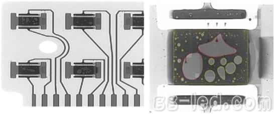
Figure 3 X-ray scan of the XM-L LED on the PCB when there are a lot of holes (> 50%)
2 thermal shock test
Thermal shock testing is one of the fastest growing forms of fatigue life testing and is a type of temperature cycle with a high rate of temperature change. The test is carried out by alternately transporting the tested product at two "chambers" of high temperature (eg 125 ° C) and low temperature (eg -40 ° C) for a specified period of time. During the thermal shock test, the solder joints experience a temperature difference of 165 ° C between high and low extreme temperatures. During the rapid temperature change, there is a large difference in expansion coefficient between different components of the assembled board. Not only does the difference in expansion coefficient cause this gravitational force, but more importantly, the temperature difference between the different components can also cause this stress. Large-area uneven expansion causes large plastic deformation of the solder joint, and the extent is far greater than the deformation that may occur in practical applications, because the temperature change is slow in practical applications. Therefore, the impact test can significantly accelerate the evolution of the failure mechanism, so that potential failure conditions can be induced in a shorter period of time.

Table 3 Thermal Shock Test Data Sheet
We observed that the XB-D LED did not fail when it reached 2000 thermal shock tests, the XP-G LED failed twice, the XM-L HVW LED failed four times, and the XM-LLED failed ten times. The thermal shock test results show that the larger LED devices with more than 50% solder voids between the LED device and the PCB have a much earlier failure time than the LED devices with less than 30% solder voids.
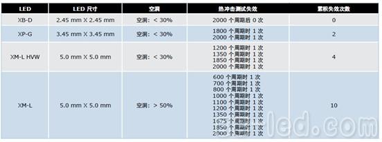
Table 4 Summary of failure conditions after thermal shock test (up to 2000 cycles)
The thermal shock data is analyzed using the Weibull distribution to understand the impact failure mechanism. In this study, the failure data of XLamp ® LEDs was modeled using a Weibull probability plot. The two-parameter Weibull distribution is defined by shape and scale parameters. The Weibull cumulative failure distribution is used to fit the number of cycles corresponding to the failure data. The formula F (N) = 1 - exp (-N/N0)m, where F (N) is the cumulative failure distribution function and N is the number of thermal cycles. N0 is a scale parameter called characteristic lifetime, that is, the number of cycles when the failure rate is 63.2%. The shape parameter m represents the shape of the Weibull curve; when m is increased, the number of failures in the loop is reduced. The shape values ​​between two and four are considered slightly normal. The shape value is less than two to form a right-inclined curve, and the shape value is greater than four to form a left-inclined curve. 
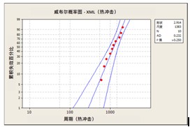
Figure 4 XP-G, XM-L HVW and XM-L LED thermal shock test, -40 ° C to +125 ° C, up to 2000 cycles
From Weibull probability plot 4, solder joints with smaller LEDs with less than 30% voids perform better than solder joints with larger LEDs with less than 30% voids. Conversely, an increase in the percentage of voids to greater than 50% results in poor solder joint performance. In addition, the characteristic lifetime of solder joints also shows a strong dependence on the degree of voids. The smaller the percentage of voids, the longer the characteristic lifetime.
3 failed solder joints
The cross section of the failed solder joint shows the presence of cracks in the solder body on the side of the component. These samples present a typical microstructure of thermomechanical fatigue failure in lead-free solder alloys. In this study, we also used a scanning electron microscope (SEM), energy dispersive X-ray (EDX) analysis, and optical microscopy to examine the solder joint interface to evaluate solder joint integrity and possible fatigue failure modes.
The performance of the solder joint after the thermal shock test is performed by performing a cross section analysis, as shown in FIG. The cross section of the failed solder joint shows that in the four LED devices, the fatigue fracture starts from the edge of the solder. Most of the fatigue cracks are present between the tin and silver particles inside the solder trace body and extend in the highest strain direction to the entire solder length.
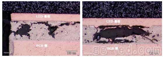
Figure 5 Solder joint between PCB and XM-L HVW LED device after thermal shock test
Cross-sectional studies have shown that there is a solder crack that extends all the way to the edge of the solder joint, and the edge of the solder joint is where the maximum stress is concentrated. These cracks occur in the inner region of the solder body, extending from one edge of the solder joint to the other, which not only reduces electrical performance, but can also cause mechanical failure of the solder joint. The XB-D LED is the smallest LED in this study. The XM-L HVW substrate is more than four times the XB-D surface area. The voids of the two LEDs are less than 30%, but studies have shown that under the XB-D LED device Solder joint cracks are not as severe as XM-L HVW. The observed cracks are typical joint fatigue fractures and are usually related to the thermal shock stress induced by the difference in thermal expansion coefficient between the dual/bonding materials.
Based on the above observations, our conclusion is that the LED device package size has a great influence on the generation of solder joint cracks. The XM-L HVW is the largest LED package size in this study. The XB-D is the smallest LED package size in this study. The voids of both LEDs are less than 30%, but studies have shown that XM- is compared with XB-D. Solder joints below L HVW have the most failure. The solder joint cracks under the larger LED device are continuous, extending from one edge of the solder to the other without interruption. The cross-sectional image shows the appearance of cracks on the component side and the PCB side. However, the degree of crack propagation on the component side is more serious.
Four conclusions
In this paper, the factors affecting the reliability of solder joints are studied. The test results show that the reliability of solder joints depends largely on the package size of LEDs and the percentage of solder voids. The more solder voids, the lower the reliability; the larger the substrate size, the less reliable the reliability. The reliability of lead-free solder joints between various sizes of XLamp ® LED devices and PCBs was analyzed by thermal shock testing from -40 °C to +125 °C. The analysis of the microstructure of the solder joint shows that the crack inside the main body of the solder joint to the side of the LED element is caused by the fatigue failure of the solder joint. The thermal fatigue failure mode is related to lead-free solder joints and is caused by the difference in thermal expansion coefficient of the material. These differences in thermal expansion coefficients are responsible for stress and mechanical strain at the material interface, which can cause fatigue cracks in the solder joints and expand.
Finally, to avoid premature solder joint failure, Cree recommends always using the recommended pad layout, solder paste, and reflow profile for XLamp ® LEDs, as detailed in Cree's related soldering and handling documentation.
Cree will participate in the Guangzhou International Lighting Exhibition on June 9-12, and the Cree booth will be located at Booth B02 in Hall 4.1 of Pazhou Exhibition Hall. More technical support and services are welcome to discuss with Cree's team in detail.
(This article is contributed by Cree)

We have been in the Lithium Battery industry for many years and always adhere to the full capacity of the product.Sufficient quantity is not false standard,ensure the power stability of lithium battery ,stable endurance. Our 3.2v 50ah LiFePo4 Battery battery have high diacharge, low battery resistance, stable discharge, longer life cycle. We have higher temperature resistance, higher power discharge.
3.2V Battery Cells,Prismatic Phosphate Lithium Batteries,3.2V 50Ah,3.2v lifepo4 battery,3.2V LifePO4 Lithium Battery Pack
Jiangsu Zhitai New Energy Technology Co.,Ltd , https://www.zhitaibattery.com