We often hear at a mobile phone conference that “×× processors are manufactured using the most advanced 10nm process.†So what does this 10nm mean? How important is nano process for CPU and SoC? What does it have to do with transistors, FinFETs, and EUV? The birth process of a CPU, in which the seventh step UV exposure is the most important lithography technology, and the lithography process is the most direct technology in the manufacturing process of the integrated circuit to reflect its advanced degree of technology, in which the resolution of the lithography technology refers to The minimum line size that the lithography system can resolve and process determines the minimum feature size of the transistors in the CPU.
According to the relevant provisions of the ITRS "International Semiconductor Technology Blueprint", the 16nm, 14nm, and 10nm that we usually talk about are used to describe the node algebra of the semiconductor process, and it should be on different semiconductor components. The objects described may be Differently, for example, in DRAM, it may be half-length Half-Pitch half-pitch length that describes the minimum allowable pitch value between two wires in a DRAM Cell; when used on a CPU, it may be described as a CPU. The minimum gate width in the transistor.
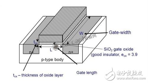
In general, the × × nm process describes the accuracy of the process under the processing scale, but it does not mean the feature size of a specific structure in the semiconductor device, but the minimum size of the processing accuracy. Here we mainly discuss the process of the CPU, because the process has an important role in CPU performance, power consumption, and heat generation. The change of the process has a great impact on the performance of the CPU. As we mentioned before, 14nm is usually used to describe the gate line width of a transistor.
Why use the gate width instead of the other line width to characterize the process node?This is mainly related to transistor structure problems. Generally speaking, the CPU internal logic gate circuit uses MosFET. It has three electrodes: gate, source, drain, and gate and source. The voltage difference between the poles can control the amount of current flowing from the source to the drain, so the gate plays a controlling role.

At the same time, the characteristics such as the transistor electron mobility are completely dependent on the doping ions and the production process, basically can not move, but the length and width ratio of the transistor gate can still be used as an article, under the same voltage, The smaller the gate width is, the electrons may flow from the negative electrode to the positive electrode through the crystal substrate, resulting in leakage, and the leakage problem will bring about a rise in static power consumption.
Therefore, the effect of the gate line width is very important. The gate line width is usually the most important parameter for designing a VLSI circuit, and therefore it is designated as the node of the semiconductor process. This is the specification of the process process in the traditional sense.
So what does this mean is that the smaller the process, the better?This is indeed the case, you think, the smaller the line width, the smaller the size of a single transistor, the smaller the area of ​​the resulting CPU dies, the same wafer can produce more CPU die, then virtually Increased vendor revenue (more tablets). In turn, you can also integrate more transistors under the same die area, and CPU performance will improve (of course, this is not absolute).
Secondly, as the gate line width becomes smaller, the operating voltage will be reduced accordingly, and the power consumption of the CPU will also be reduced. In addition, under more advanced processes, the transistor cut-off frequency will perform better, and the CPU will naturally work. At a higher frequency. So we often see that SoC, CPU, we have adopted a more advanced 10nm, power consumption has decreased × ×%, the frequency has increased × ×%, performance has increased × ×%.
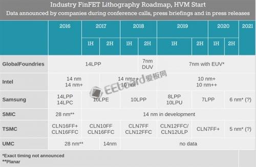
Taiwan Semiconductor Manufacturing Co., Ltd. has been mass-produced for 10nm for a long time. Intel has not shipped yet. Intel's invincible process has failed.In the past few years, Intel entered the 14nm era from 22nm. Everyone was saying that Intel was at least three to five years ahead of other manufacturers in the process. However, it was not long ago. We found that Intel 14nm actually polished again and again from Skylake. (14nm), Kaby Lake (14nm+), Coffee Lake (14nm++), still in use after three generations, it is said that there will be 14nm + + +, originally said that a good 10nm suffered a large number of technical problems and dystocia.
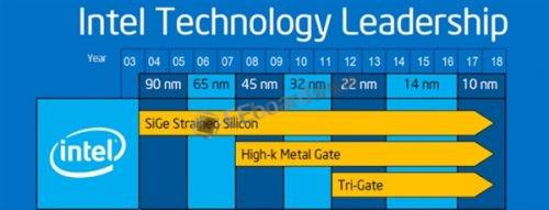
On the other hand, rivals TSMC and Samsung are making waves on the OEM circuit, catching up with Intel's progress on the 16/14nm node. Surprisingly, Taiwan Semiconductor Manufacturing Co. and Samsung's 10nm process mass production is far earlier than Intel's. Related products (such as (Qualcomm Xiaolong 835) Even after it had been sold on the market for a full year, TSMC even mass-produced a 7nm chip this year. What is going on here?
The general public believes that 10nm is certainly more advanced than 14nm, and 12nm is better than 14nm. When Intel was overwhelmed by negative public opinion voice, Intel broke through the "mystery" behind the number of nanometer process technology, because TSMC and Samsung's process numbers have been different. The degree of "beautification" is a little clever in terms of naming, that is, "digital" suppression. Although Intel loses in "digital", Intel is actually superior to some key technical parameters in all aspects of the process. This phenomenon has occurred in the previous 14nm, and the ××nm process has begun to break away from its original scope. Everyone begins to “counterfeitâ€.
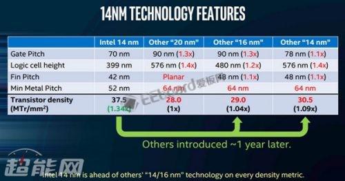
14nm era, Intel has kicked off a behind-the-scenes secret
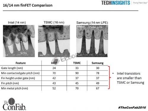
Techinsights also made a comparison, Intel 14nm is indeed better than Samsung's 14nm LPE
Intel indicated that the line width only represents the process node, but to measure the quality of the process, Gate Pitch gate spacing, Fin Pitc fin spacing, Fin Pitch minimum metal spacing, Logic Cell Height logic cell height parameters more reference significance. At the same time, Mark Bohr, Senior Director of Intel's Processor Architecture and Integration Division, proposed to measure the semiconductor process level with Transistor Density transistor density, and proposed the following formula:
For example, at the Technology and Manufacturing Day held by Intel in September last year, it unveiled three technical parameters related to the 10nm process. We have seen that Intel has suspended the other two in these key technical indicators, such as Intel's 10nm light. The gap between the fins and the gates produced by the engraved technology is smaller (note that Intel has published the interval comparison, not the line width, and it is more significant). As a result, transistor density is almost twice that of TSMC and Samsung, reaching 100 million transistors per square millimeter, while maintaining a good tradition of low logic cell height, and has an advantage in 3D stacking.
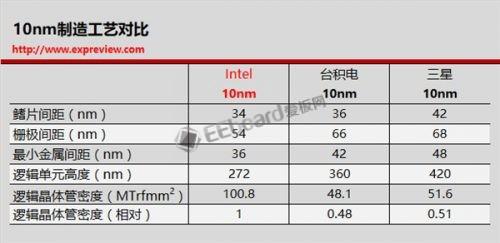
Recently, Semiwiki reported on Samsung's 10nm, 8nm, and 7nm process transistor density. The transistor densities for the 10/8/7nm process are 55.10/64.4/101.23 MTr/mm2, respectively. It can be seen that Samsung's 7nm process is only able to trace Intel’s 10nm on transistor density, and who is playing tricks, don’t you not know?
Where is the limit of that process?When the process is less than 20nm, because the silicon dioxide insulating layer is too thin, and only a few atoms are so thick, then this time is very unstable for the transistor, which will cause electrons to randomly pass through the barrier and cause leakage, resulting in chip work. Increased consumption. However, this is still a minor problem. Intel has developed high-k film and metal gate ICs, as well as the familiar FinFET fin field-effect transistor structure. By increasing the surface area of ​​the insulating layer to increase the capacitance, the leakage current can be reduced. problem. At the same time, in order to create a 7nm line width, the industry consensus is to use EUV EUV as a lithography light source, with few exposure times, not to overcome the optical proximity correction characteristics caused by diffraction effects, but there are still a lot of problems, so EUV lithography technology has not yet Fully mature.
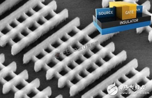
When the process progresses to 7nm, semiconductor companies are even less calm, because on silicon-based semiconductors, the linewidth of transistors has dropped to 7nm. An inevitable problem has occurred, the well-known quantum tunneling effect.
In classical physics, when the energy of a macroscopic particle is less than the height of a barrier, it is impossible for this particle to cross this barrier, but for a microscopic particle, with wave-particle duality at this time, the magical quantum effect appears, even if Energy is below the barrier height and there is still a certain probability that it can break through the barrier. This will cause a big problem. The electronics have passed in the end. If there is no monitoring, the logic gate outputs 0 or 1, and the answer does not know. Then the CPU will not work properly. Therefore, this problem should be eliminated.

Leading semiconductor manufacturing companies such as Intel, Taiwan Semiconductor Manufacturing Co., and Samsung have conducted research on this issue. There are still some measures to prevent the quantum tunneling effect. For silicon-based semiconductors, Intel is looking forward to the process limit is 5nm or 3nm; Samsung will then follow the 8/7/6/5/4nm LPP process, and will introduce the Multi Bridge Channel FET structure at 4nm (abbreviated MBCFET, multi-channel field Effector), a unique GAAFET (Logic Gate Around Field Effect Transistor) technology, uses two-dimensional nano-lamellas to overcome the limitations of physical expansion and FinFET architecture.
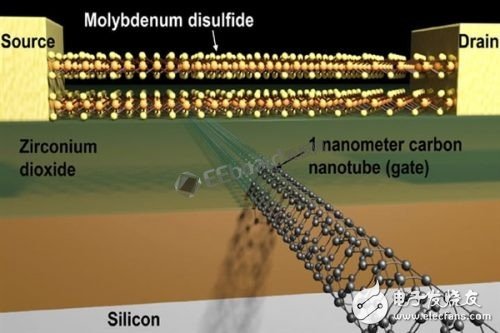
The reports on the media below 3nm process are not based on silicon oxide, but rather new composite semiconductor materials such as graphene, and all of them are laboratory technology breakthroughs that cannot be mass-produced in a short time. However, looking for new materials instead of silicon for lower process transistors is one of the most effective solutions.
The False and Reality Behind Nano-Process ProcessAfter reading the full text, you will know that the so-called 10nm and 7nm semiconductor processes have deviated from the original category. They are no longer strictly line widths. The 16nm “optimization†can be called 12nm, and the 10nm “optimization†can also be called 8nm. As an advocate of Moore's Law, Intel is certainly overwhelmed. He repeatedly commented on Samsung and TSMC’s “digital beautification†behavior. Actually from the transistor density parameters, Samsung's 7nm ≈ Intel 10nm, so it seems that Intel's 10nm dystocia is extenuating, the goal is set too high, but was a friendly business to win a name to win, the general public actually Because I do not understand the actuality of the manufacturing process and believe the vendor side. Intel's manufacturing process technology is not so unbearable, it is still in the world's leading position.
The 7-inch tablet can be used as the golden size of a tablet computer. It is small and portable. It can be used at home and outdoors. You can browse the web, watch videos and play games. It is a household artifact. Although the size of the 7-inch tablet is inclined to the tablet, the function is more inclined to the mobile phone, so it can also be used as a substitute for the mobile phone. Compared with other sized tablets, the 7-inch tablet has obvious advantages in appearance and weight. Both the body size and the body weight have reached a very reasonable amount.
1.In appearance, the 7 inch tablet computer looks like a large-screen mobile phone, or more like a separate LCD screen.
2.In terms of hardware configuration, the 7 inch tablet computer has all the hardware devices of a traditional computer, and has its own unique operating system, compatible with a variety of applications, and has a complete set of computer functions.
3.The 7 inch tablet computer is a miniaturized computer. Compared with traditional desktop computers, tablet computers are mobile and flexible. Compared with Laptops, tablets are smaller and more portable
4.The 7 inch tablet is a digital notebook with digital ink function. In daily use, you can use the tablet computer like an ordinary notebook, take notes anytime and anywhere, and leave your own notes in electronic texts and documents.
7 Inches Tablet Pc,Quad Core Tablet 7 Inch,7 Inch Gaming Tablet,Supersonic Tablet 7 Inch
Jingjiang Gisen Technology Co.,Ltd , https://www.gisengroup.com