The first chapter is the AM824-Core development kit . This article is 1.3 Switch Matrix (SWM) and 1.4 AM824-Core .
1.3 Switch Matrix (SWM)
> > > Â Â 1.3.1 Introduction to SWM
The Switch Matrix shown in Figure 1.4 is a very unique peripheral function integrated in the MCU by NXP. Through the switch matrix, all digital peripheral function pins in the chip can be assigned to the power supply. Any pin outside the ground, which increases the flexibility of the design.
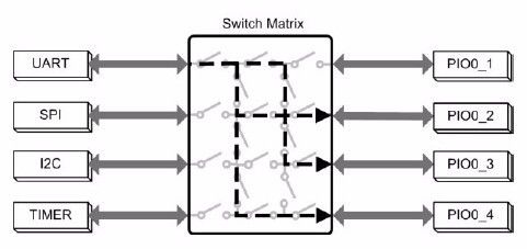
Figure 1.4 SWM function diagram
Due to the existence of the switch matrix, the peripheral function pin signals of the LPC824 can be divided into fixed function signals and assignable digital signals. The corresponding peripheral functions are as follows:
Fixed function signal
GPIOx, RESET, VDDCMP, ACMP_I1~ACMP_I4, ADC_0~ADC_11, SWDIO, SWCLK, XTALIN, XTALOUT, CLKIN, and standard I2C open-drain pins I2C0_SDA and I2C0_SCL, these function pins are fixed at a pin position outside the chip. Cannot be assigned to other external pins through SWM.
Assignable digital signal
USART0, USART1, USART2, SPI0, SPI1, CTIN, CTOUT, I2C1, I2C2, I2C3, ACMP_O, CLKOUT, these signals can be assigned to any external pin other than power/ground via SWM.
> > > 1.3.2 SWM Application
Since some of the MCU's digital peripherals can be assigned to other pins of the chip as needed, the user's design will be greatly simplified. which is:
(1) When designing the system hardware, the peripheral device layout and PCB layout are the mainstays, and the pin position of the signal is not considered, which helps to alleviate the congestion of the PCB and reduce the development cost;
(2) When replacing system peripheral devices or main controllers, avoid changing hardware design and reducing maintenance costs;
(3) Assign multiple functions to the same pin to implement special functions (use with caution).
Below we will actually experience the characteristics of SWM in a few small cases in practical applications.
1. Solve hardware design errors
In the user circuit design process, there are often some unexpected errors, such as the serial connection between the serial host and the TXD pin of the device (actually cross-connected), which causes the PCB to be redesigned, increasing the design cost of the product. If the main controller supports SWM Function, even if the PCB design is wrong, you can ensure the function is normal without modifying the hardware.
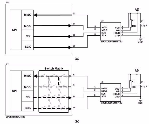
Figure 1.5 Solving Hardware Design Errors
Figure 1.5 (a) shows the application circuit of the MCU driving SPI Flash, but the circuit design error can be found. The MOSI/MISO pin of the SPI Flash and the corresponding pin of the MCU should be directly connected, and the actual circuit uses a cross-connection. Therefore the circuit cannot be used directly. If the MCU in Figure 1.5(a) is the LPC824, the SWM can be flexibly implemented to redistribute the SPI peripheral pin function signals without redesigning the hardware. See Figure 1.5(b).
2. Simplify peripheral design
Communication problems with different voltage signals in system applications are often encountered. The more common ones are 3.3V system and 5V system compatibility issues. For example, 3.3V system products communicate between serial and 5V system products, requiring TXD and RXD pins. After level conversion, reliable communication is possible.
The power supply range of the LPC824 is 1.8 V~3.6 V. It usually works in a 3.3V power supply environment. If the LPC824-based product needs to support 5V serial communication, the serial communication interfaces TXD and RXD of the LPC824 need to be processed to be external. The 5V system is connected, and this part of the circuit can be level-shifted by multiple discrete devices or level-shifting chips, which increases design complexity and increases design cost. However, the 8th and 9th pins of the LPC824 are standard open-drain pins (the I2C0_SDA and I2C0_SCL pins of the default I2C 0 are assigned to this pin). In practice, the TXD and RXD of the UART can be assigned to this via SWM. At the two pin positions, the 5V level is directly compatible with the external pull-up resistor to the 5V power supply, which simplifies the peripheral design and implements the corresponding functions. See Figure 1.6 for details.
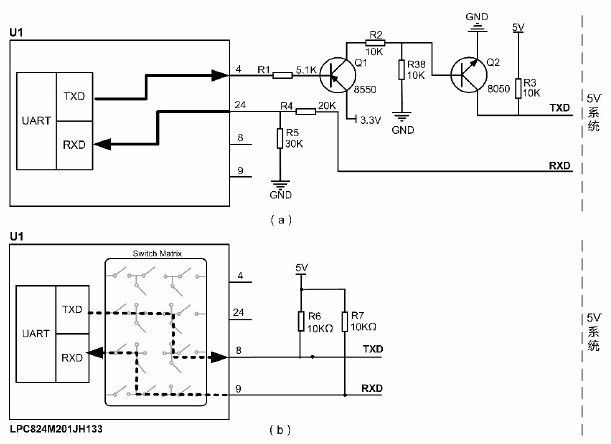
Figure 1.6 Flexible application of SWM
1.4 AM824-Core
The AM824 development kit includes the AM824-Core and MiniCK100 emulators. Figure 1.7 shows the AM824-Core diagram. The MCU is the NPC semiconductor LPC824M201JHI33, which includes two MiniPort interfaces, one MicroPort interface, and one 2×10 expansion interface. These interfaces not only bring out all the I/O resources of the MCU, but also extend the various modules with the MiniPort interface and the icroPort interface. On-chip resources include 2 LEDs, 1 passive buzzer, 1 heating resistor, 1 LM75B temperature measurement chip, 1 thermistor, 1 TL431 reference source, 1 multi-function independent button and 1 Reset the button to complete a variety of basic experiments.
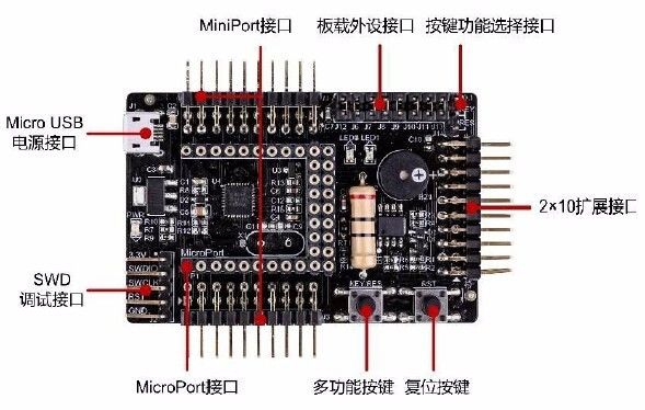
Figure 1.7 AM824-Core development board interface distribution
The emergence of the AM824-Core simplifies the user's hardware design, making the learning of the LPC824 series MCUs much less difficult, helping beginners quickly master application development based on 32-bit CortexTM-M0+ core microcontrollers.
> > > Â Â 1.4.1 Power Circuit
1. System power
The AM824 is powered by a 5V USB and needs to be converted to 3.3V for the LPC824. In order to achieve 5V to 3.3V conversion, AM824 chose SPX1117M3-L-3.3V power management device from EXAR Semiconductor Company. The input voltage is 4.7V~10V, the maximum input current is up to 800mA, and the typical voltage difference is 1.1V when the load is 800mA.
The typical application circuit of SPX1117M3-L-3.3V in SOT223 package is shown in Figure 1.8. The input and output terminals of the chip are connected with two filter capacitors respectively. The filter capacitor ensures the stability of the voltage to reduce the glitch interference.
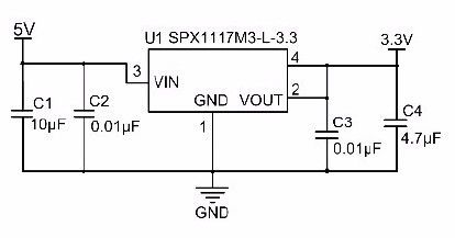
Figure 1.8 LDO Typical Application Circuit Diagram
The AM824-Core has a standard Micro-USB interface, which you can usually see on mobile phones, mobile charging treasures and other devices. Because the LPC824 does not support USB communication, this interface is mainly used for power supply, and can provide 5V power through devices such as mobile phone chargers or computers.
Micro-USB is a USB 2.0 standard interface and is the next version of Mini-USB. Its characteristics are as follows:
The Micro-USB connector is smaller than standard USB and Mini-USB connectors, saving space;
With up to 10,000 insertion and removal life and strength;
Blind insertion structure design;
Compatible with USB1.1 (low speed: 1.5Mb/s, full speed: 12Mb/s) and USB 2.0 (high speed: 480Mb/s);
Both data transmission and charging are provided.
2. Reference source circuit
The on-board reference chip of the AM824-Core development board is the TL431, which is a commonly used controllable precision regulator. Its main features are as follows:
Programmable output voltage: 2.5V~36V;
Voltage reference source error: typically +/- 0.4% @ 25 ° C;
Low dynamic output impedance, typically 0.22 Ω;
1.0mA to 100mA sink current capability.
The circuit for outputting the 2.5V reference voltage of TL431 is shown in Figure 1.9. R13 is a current limiting resistor to ensure that the current input to the TL431 is within 1~100mA.
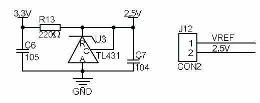
Figure 1.9 Reference source circuit
> > > Â Â 1.4.2 Minimum system
The minimum system circuit of the LPC824 microcontroller mainly includes two parts, the reset circuit and the clock circuit. See Figure 1.10 for details. Since the ILC clock is integrated inside the LPC824 chip, the external clock circuit can be omitted.
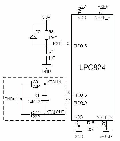
Figure 1.10 Minimum System Circuit
When the system requires a more accurate clock signal, an external clock circuit can be used. The recommended clock circuit uses a 12MHz external crystal and capacitors C9 and C11 to form an oscillator circuit.
> > > Â Â 1.4.3 Reset and Debug Circuit
1. Reset circuit
Internal reset circuit
If the requirements are not high, for example, directly driving the LED digital tube and keyboard scanning circuit, the internal reset circuit can be selected. Or the internal reset circuit can be used in cases where the interference is not serious.
RC reset circuit
Computer systems have logic, and the state of some logic circuits is unpredictable when the power is turned on. Therefore, in order for a digital device or computer to work properly, it is necessary to make the output of all logic circuits in the system at a specified high or low state at power-on, which is the function of the reset circuit. The reset circuit enables the device to automatically generate a high or low pulse signal with a certain width immediately after power-on and after the power supply voltage is stable.
Using the charge-discharge delay principle of the capacitor, the reset pulse signal required by the MCU at power-on can be generated. As shown in Figure 1.11, the circuit schematic diagram for generating a low-level reset signal is shown. In Figure 1.11, when the MCU is powered up, VC remains low because the voltage VC across capacitor C cannot be abrupt. However, as the capacitor C is charged, the VC continues to rise, and the rising curve is shown in Figure 1.11. As long as the appropriate R and C are selected, the VC can continue to reset the MCU for a sufficient time below the MCU reset voltage. After reset, VC rises to the supply voltage and the MCU starts to operate normally. Equivalent to a low-level pulse signal of a certain width when the MCU is powered on, which resets the MCU.
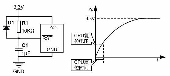
Figure 1.11 RC reset circuit diagram
Figure 1.12 shows the RC reset circuit of the AM824-Core. The role of D2 is to provide a fast discharge circuit for capacitor C1 when the power supply voltage disappears, so that the voltage at the reset terminal can be quickly reset to zero, so that it can be powered up next time. Reliably reset. After shorting J8, manual reset can also be achieved by the reset button.
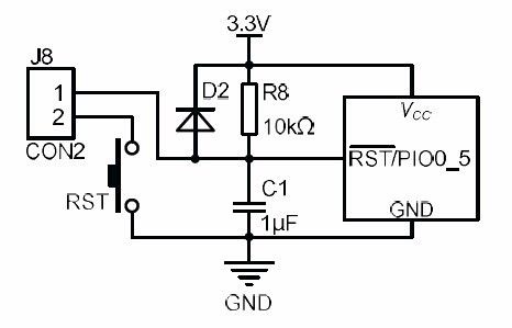
Figure 1.12 Reset Circuit
2. Debug circuit
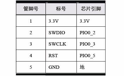
The AM824-Core brings up the SWD debug interface. Compared with the JTAG debug mode, the SWD debug mode is faster and uses fewer I/O ports. Therefore, the AM824-Core development board leads to the SWD debug interface. The reference circuit is shown in Figure 1.13. For details on the pin function, see Table 1.5.
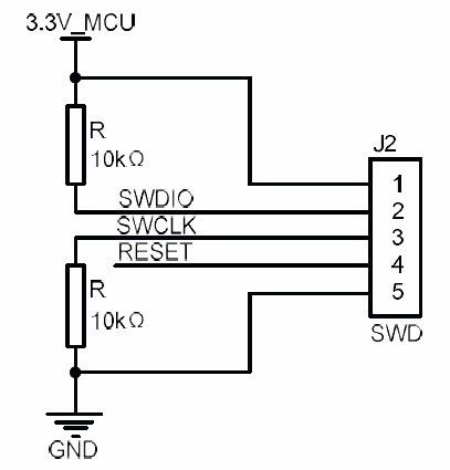
Figure 1.13 Debug Circuit
Table 1.5 Description of Debug Pins
> > > 1.4.4 Onboard peripheral circuits
1. LED circuit
The AM824-Core development board has two LED light-emitting diodes for simple display tasks. The circuit is shown in Figure 1.14. The pin numbers GPIO_LED0 and GPIO_LED1 correspond to PIO0_8 and PIO0_9. The LED is active low (active low). . The control pins of the LED circuit are connected to the I/O pins of the microcontroller via J9 and J10. R3 and R4 in the circuit are the current limiting resistors of the LED. Selecting a value of 1.5kΩ can avoid over-brightness when the LED is lit.
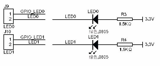
Figure 1.14 Onboard LED Circuitry
2. Buzzer circuit
For ease of debugging, the AM824-Core has designed a buzzer driver circuit, as shown in Figure 1.15. The pin number PIO_BEEP corresponds to PIO0_2. The AM824-Core development board uses a passive buzzer. D1 acts as a protection triode. When a sudden cutoff occurs, the instantaneous induced electromotive force generated at both ends of the passive buzzer can be quickly released through D1 to avoid superposition on the collector of the triode. Thus breakdown. If an active buzzer is used, D1 is not soldered. When the buzzer is not used, you can also disconnect the buzzer circuit from the I/O port with J7.
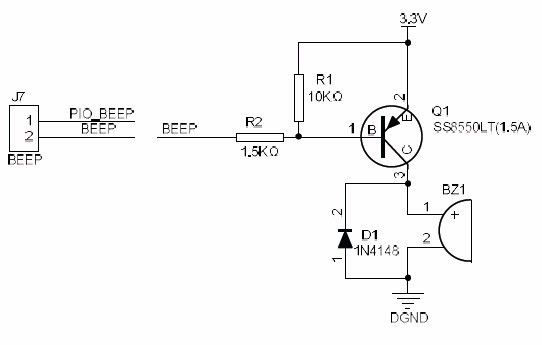
Figure 1.15 Onboard Buzzer Circuit
3. Heating resistor and button circuit
The AM824-Core development board innovatively designed a temperature measurement experiment circuit. Includes heating circuitry and digital/analog temperature measurement circuitry. The heating circuit uses a power resistor (2W) with a resistance of 20~50Ω, which is controlled by the button. See Figure 1.16 for details. The pin number GPIO_KEY corresponds to PIO0_1. The smaller the resistance is, the larger the current is, and the greater the heat generated. Therefore, if the R32 is soldered with a small resistance, it is not suitable for heating for too long. The function of the button needs to be selected as the heating button with the jumper cap on J14. When the button is pressed, the circuit is turned on, and the heat generated by the resistor causes the temperature around the resistor to rise. At this time, the temperature rise circuit can be observed through the temperature measuring circuit.
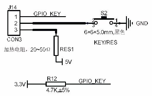
Figure 1.16 Heating circuit
4. Digital temperature measuring circuit
The AM824-Core selects the LM75B as the main chip of the digital temperature measurement circuit. The LM75B is fully compatible with the LM75A, but the static power consumption is slightly lower. The circuit is shown in Figure 1.17. The pin numbers PIO_SDA and IO_SCL correspond to PIO0_11 and PIO0_10. The LM75B is a temperature-to-digital converter with a built-in bandgap temperature sensor and sigma-delta analog-to-digital conversion. It is also a temperature detector and provides overheating output.
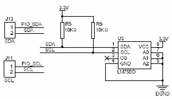
Figure 1.17 LM75B circuit
The main features of the LM75B are as follows:
Temperature accuracy up to 0.125 ° C accuracy;
Wide supply voltage range: 2.8V~5.5V;
Ambient temperature range: Tamb=-55°C~+125°C;
Lower power consumption, the current consumed in shutdown mode is only 1μA;
I2C bus interface, up to 8 devices can be connected on the same bus.
In circuit design, R5 and R6 are pull-up resistors for the I2C bus. Since there is only one LM75B on the board, regardless of the address of the chip, the A0~A2 pins of the chip can be directly grounded. The OS is the overheating output of the chip. It can realize the function of an independent temperature controller by external relays. Since the temperature control is controlled by the single chip microcomputer, this pin can be omitted.
5. Analog temperature measurement circuit
The analog temperature measurement circuit is measured by the electrical specific temperature change characteristics of the thermal element. The AM824-Core development kit selects the thermistor as the temperature measurement element, and the thermistor uses the MF52E-103F3435FB-A. The range is from 0 to 85 ° C, and the resistance varies from 27.6 to 1.45 KΩ. The temperature measurement circuit is shown in Figure 1.18. The pin number PIO_ADC corresponds to PIO_14. It uses a simple resistor divider circuit, of which C8 is for the circuit output to be more stable. The MCU collects the voltage value on the voltage dividing resistor through the ADC. When the temperature changes, the resistance value of the thermistor changes, and the ADC value collected by the MCU also changes. By calculating the resistance value of the thermistor, and comparing the resistance table of the thermistor with the temperature, the current temperature value can be obtained.
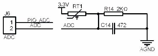
Figure 1.18 Thermistor Circuit
> > > Â Â 1.4.5 Jumper cap use
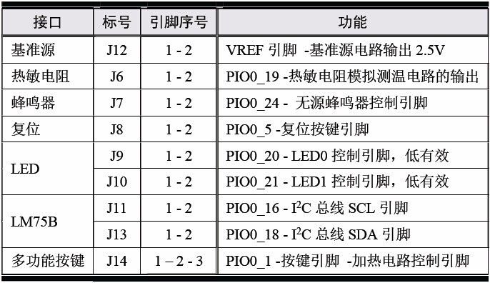
The onboard peripheral interface is designed between the MCU pins and the onboard peripheral circuitry and can be shorted by a jumper cap, as shown in Figure 1.19. This design is designed to allow peripheral circuits to be disconnected from the MCU pins when not in use, without affecting these pins for other functions. See Table 1.6 for details.
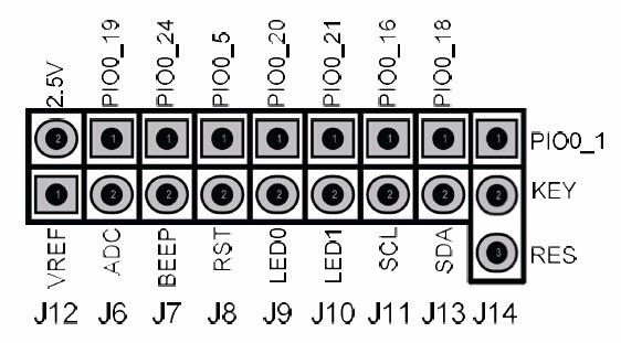
Figure 1.19 Onboard Peripheral Interface Pin Diagram
Table 1.6 Onboard Peripheral Interface Pin Description
> > > Â Â 1.4.6 MiniPort Interface
The MiniPort (2×10) interface is a universal onboard standard hardware interface that can be connected to the standard modules to further simplify hardware design and expansion. Its characteristics are as follows:
Using a standard interface definition, a 90° curved needle with a 2×10 pitch of 2.54 mm is used;
Multiple expansion interface modules can be connected at the same time;
Has 16 general purpose I/O ports;
Support 1 SPI interface;
Support 1 channel I2C interface;
Support 1 UART interface;
Supports one 3.3V and one 5V power interface.
The function description of the standard MiniPort (2×10) interface is shown in Figure 1.20. The connector used in the MiniPort (2×10) interface is 2×10 pin/mother (90°) with 2.54mm pitch. The package style is shown in the figure. 1.21. The main controller backplane selects the 90° pin header, the function module selects the 90° busbar to connect with the host, and uses the 90° pin header to pull all the pins out to realize the horizontal stacking of the modules.
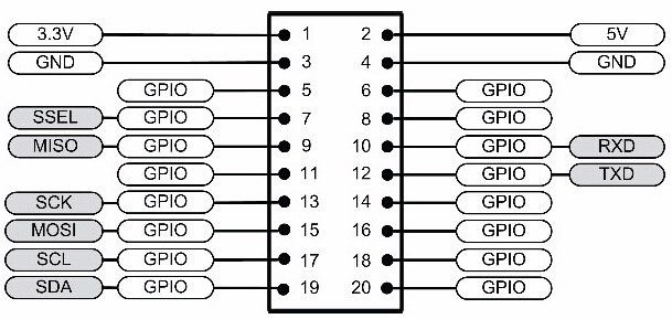
Figure 1.20 MiniPort (2×10) interface function description

Figure 1.21 MiniPort (2 × 10) interface connector
The connection between the 90° pin header of the MiniPort and the 90° pin header, A1 - B20, A2 - B19 ... A19 - B2, A20 - B1 (A stands for pin header and B stands for pinch). MiniPort (2×10) currently supports MiniPort-Key, MiniPort-LED, MiniPort-View and MiniPort-595. These modules can be directly plugged into MiniPort, and can be connected to various development boards through DuPont.
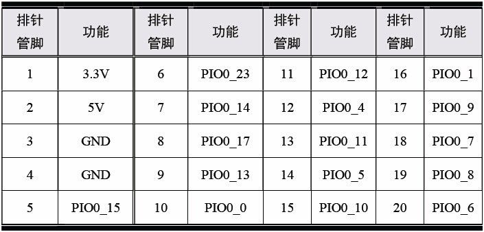
The AM824-Core development board is equipped with two MiniPorts with interfaces J3 and J4. The J3 and J4 interface pins are exactly the same, and the user can choose to use according to the custom. The specific pin assignment is shown in Table 1.7.
Table 1.7 MiniPort Pin Assignment
> > >   1.4.7 2×10 Extended Interface Description
The LPC824M201JHI33 has 33 pins and 29 I/O pins. Since MiniPort only defines 16 I/Os, there are still some I/Os that are not exported.
In order to expand the peripheral interface, all the remaining pins need to be taken out. Based on this, a 2×10 expansion interface is also designed for the M824-Core, which not only extracts the unused I/O of the MiniPort, but also includes a set of power supplies. The interface and a reference source pin (VREF) are shown in Figure 1.22.
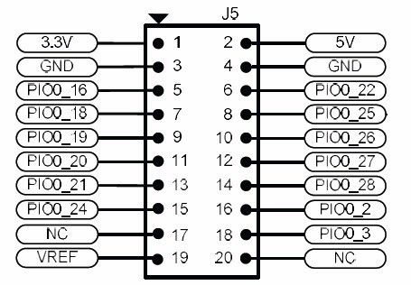
Figure 1.22 2×10 Expansion Interface Pin Diagram
> > > 1.4.8 MicroPort Interface
In order to facilitate the expansion of the development board functions, ZLG has developed the MicroPort interface standard. MicroPort is a hardware interface dedicated to extended function modules, which effectively solves the connection and expansion between the device and the MCU. Its main features are as follows:
Has a standard interface definition;
The interface includes a wealth of peripheral resources supporting UART, I2C, SPI, PWM, ADC, and DAC functions;
The supporting function modules will be more and more abundant;
Support for stacking up and down.
MicroPort is divided into standard interface and extended interface. The extended interface can implement richer peripheral applications. Different interface types can be selected in different application environments. The connector used in the MicroPort interface is a 1×9 round hole pin with a 2.54 pitch and a height of 7.5 mm for stacking up and down. MicroPort is divided into standard interface and expansion interface. The MicroPort standard interface is U-shaped with 9 pins on each side and 27 pins. The pin function definition is shown in Figure 1.23. The MicroPort standard interface contains 22 I/O pins for up to 1 UART, 1 I2C , 1 SPI, 2 ADCs, 1 DAC, and 4 PWM functions, all of which can be used as normal I/O. The MicroPort standard interface also includes a 3.3V, 5V voltage pin and a VREF (reference reference source) pin, as well as a reset pin for the MCU.
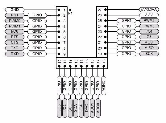
Figure 1.23 MicroPort Standard Interface Pin Definition
The MicroPort expansion interface is based on the MicroPort standard interface. A row of 1×9 pins is added to the bottom of the U-shape. These 9 pins can lead to SDIO and USB expansion interfaces, and can also be used as normal I/O. For some MCUs, due to the rich pin resources, more modules can be supported by the MicroPort expansion interface to achieve more expansion functions. The pin definitions added to the MicroPort expansion interface are shown in Figure 1.24. The SDIO interface of the MicroPort expansion interface is four-wire, and the USB interface can support OTG mode.
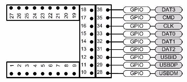
Figure 1.24 Pin Definition Added by MicroPort Expansion Interface
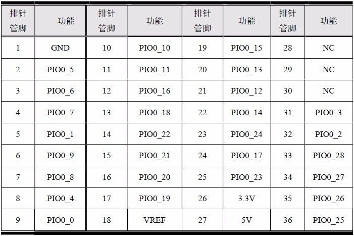
The AM824-Core has an onboard 1 port with an extended MicroPort interface. Users can select or develop a variety of MicroPort modules to quickly and flexibly build prototypes. Due to the limited on-chip resources of the LPC824, there are very few pins that are defined by the MicroPort interface. The corresponding pins can be used as normal I/O. The pin assignment of the MicroPort interface of the AM824-Core is shown in Table 1.8.
Table 1.8 AM824-Core MicroPort Pin Assignment Table
Wired Headphone,Wired Gaming Headphones,Wired In Ear Headphones,Wired Bluetooth Headphones
Guangzhou YISON Electron Technology Co., Limited , https://www.yisonearphone.com