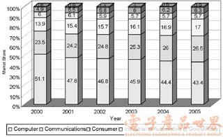
Figure 1 Changes in market share of global semiconductor application products from 2000 to 2005

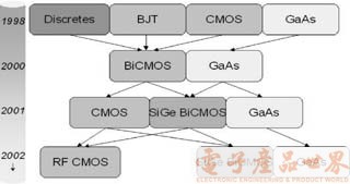
Figure 2 Wireless communication IC process technology development process

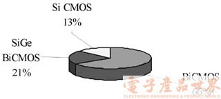
Figure 3 Estimated market share of mobile phone transceivers in 2004

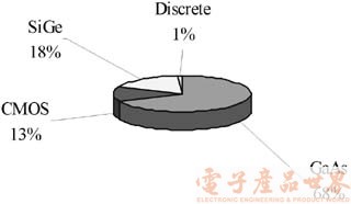
Figure 4 Estimated market share of mobile phone power amplifiers in 2004 (by process)
Foreword The application of semiconductors can be divided into the computer, communications, consumer electronics, industrial, automotive, and military markets. According to statistics from the Semiconductor Industry Association and research institute IC Insight, since 2001, computers have been in the semiconductor application product market. The occupancy rate has started to fall below 50%. In contrast, the occupancy rate of communications and consumer electronics products has increased year by year, becoming an important product that drives the continued growth of the semiconductor industry (see Figure 1). Among them, in the communications market, the mobile phone market with an annual output of about 400 million units is currently the focus of major semiconductor manufacturers. For example: TSMC and UMC, two of the world's largest wafer foundries, competed to announce in the 2002 technology forum The blueprint of the new process technology applicable to wireless communication ICs shows that wireless communication ICs have become an important pillar for the future development of the semiconductor industry.
Generally speaking, the entire wireless communication IC can be divided into three parts according to its functions: firstly, it is a radio frequency IC (Radio Frequency IC) responsible for receiving / transmitting radio frequency signals. This part belongs to the radio frequency front end and is designed for pure analog circuits; secondly, it is responsible for secondary Intermediate frequency circuit (IF IC) with up / down frequency and modulation / demodulation functions, as well as components such as phase-locked loop (PLL), frequency synthesizer (Synthesizer), etc. At present, this segment mostly belongs to analog / digital mixed mode (mixed mode) ); The last is the baseband IC (baseband IC) responsible for pure digital parts such as A / D, D / A, signal processor and CPU.
Since the fundamental frequency part is mainly used to process digital signals, and its internal components are mostly active components, the distribution of lines is extremely dense, so it has always been based on the miniaturization and high integration of pure silicon CMOS processes. In the radio / intermediate frequency part, because wireless communication has strict requirements on the specifications of RF ICs, and the functions of high-frequency transistors are different, their circuit design concepts are also different. Therefore, how to choose different materials and processes to enable wireless communication It is often the most important issue for the manufacture of integrated circuits for wireless communications to achieve balance or optimization of circuit functions and prices of integrated circuits. Therefore, this article will focus on the process technology of wireless communication RF IC to discuss the development focus and trend of semiconductor process technology in the field of wireless communication RF IC.
Overview of Semiconductor Materials and Processes for Wireless Communication Semiconductor materials can be divided into element semiconductors composed of a single element and compound semiconductors composed of more than two element compounds. The former is a semiconductor formed by silicon, germanium and the like, and the latter is a semiconductor formed by compounds such as gallium arsenide (GaAs) and indium phosphide (InP). In the past, when personal computers were the main axis of application, the global semiconductor industry has focused on the development of silicon materials. Due to the inherent physical limitations of silicon, the traditional complementary metal oxide semiconductor (CMOS) process is incapable of handling high-frequency signals above 1 GHz, making the demand for semiconductors for communications in the past two to three years particularly rapid. For wireless communication ICs with extremely strict requirements for high operating frequency, high amplification rate, and low noise, the demand for special semiconductor materials and manufacturing processes is particularly valued (see Figure 2). Under the continuous efforts of the industry, R & D processes that can be applied to wireless communication ICs include: silicon bipolar complementary metal oxide semiconductor (Si Bipolar CMOS), silicon germanium (SiGe), gallium arsenide (GaAs), and others Different processes such as indium phosphide or E-mode pHEMT are still under active development. In the following, further explanations will be provided for these semiconductor materials and processes (as shown in Table 1).
Silicon components â— Si BiCMOS is the mainstream silicon-based integrated circuit. There are Si BJT (Si-Bipolar JuncTIon Transistor), Si CMOS, and Si BiCMOS (Si Bipolar Complementary Metal Oxide Semiconductor) combining Bipolar and CMOS characteristics. Since silicon is the most mature material currently used in the semiconductor industry, it has great advantages in terms of output and price. Traditionally, the transistors made of silicon mostly use BJT or CMOS. However, because the silicon material does not have a semi-insulating substrate, and the gain of the component itself is low, if it is to be applied to the manufacture of wireless communication ICs operating in high frequency bands, further To improve its high-frequency electrical properties, in addition to improving the material structure to increase the fT of the device, it is also necessary to use trench isolation and other processes to improve the isolation and Q value between the circuits. In this way, the process will be more complicated, and The defect rate and cost will also increase significantly. Therefore, at present, the Si BiCMOS process with low noise, fast electron movement and high integration is mainly used. The main applications are mainly IF modules or low-level RF modules. As for the manufacture of RF front-end components such as low-noise amplifiers, power amplifiers and switches, it is still inadequate.
â— SiGe process is emerging
In the 1980s, IBM added Ge to improve Si materials in order to increase the speed of electron flow, reduce energy consumption and improve functions, but unexpectedly successfully combined Si and Ge. Since IBM announced that SiGe has entered the mass production stage in 1998, SiGe has become one of the most valued wireless communication IC process technologies in the past two or three years.
In terms of material characteristics, SiGe has good high-frequency characteristics, good material safety, good thermal conductivity, mature process and high integration, and has the advantage of lower cost. In other words, SiGe can not only directly use the existing semiconductor 200mm wafer process , To achieve a high degree of integration, based on the creation of economic scale, and high-speed characteristics comparable to GaAs. With the recent investment of large IDM manufacturers, SiGe technology has gradually been improved in the problems of cutoff frequency (fT) and breakdown voltage (Breakdown voltage) is too low and become increasingly practical. At present, this process technology developed by IBM has integrated high-efficiency SiGe HBT (HeterojuncTIon Bipolar Transistor) 3.3V and 0.5μm CMOS technology, can use active or passive components, engaged in analog, RF and mixed signal aspects Configure the application.
For wireless communication RF IC applications, SiGe technology has good linearity, low noise, fast and other characteristics, can be applied to mobile phone RF front-end such as LNA, Mixer, etc. Therefore, with the increasingly perfect performance of SiGe process technology, coupled with high integration, global RF chip manufacturers and wafer foundry manufacturers have successively invested in the development of this technology.
â— RF CMOS is ready to go although the pure silicon CMOS process is considered to be only suitable for designs with more digital functions, but not for RF IC designs based on analog circuits. However, after more than ten years of efforts, With the improvement of CMOS performance, the cooperation of wafer foundries under 0.25mm process technology, and the trend of wireless communication chip integration, RF CMOS process is not only a hot topic in academic research, but also aroused industry attention. The biggest advantage of using the RF CMOS process is, of course, a high degree of integration that can combine radio frequency, fundamental frequency and memory components, and at the same time reduce component costs. But the crux of the problem still lies in whether RF CMOS can solve the problems of high noise, low insulation and Q value, and the increase in process cost by reducing the performance improvement, so as to meet the strict requirements of wireless communication RF circuits.
Currently, RF CMOS has been used to produce RF ICs, and most of the products have Bluetooth and WLAN RF ICs with relatively loose RF specifications. For example, Bluetooth chip manufacturers such as CSR, Oki, Broadcom, etc. have launched Bluetooth transmitters using CMOS; Atheros, Envara WLAN chip manufacturers have also recently launched multi-mode WLAN (.11b / g / a) RF chipsets with a full CMOS process. However, due to the very strict specifications of radio frequency ICs for mobile phones, so far, in addition to Silicon Labs using digital technology to strengthen the low-IF to baseband filter and digital channel selection filter functions to reduce the problem of excessive CMOS noise. In addition to low-IF GSM / GPRS chipsets, few manufacturers use this technology to make mobile phone RF ICs. In addition, because mobile phone manufacturers still have deep doubts about their reliability, apart from South Korea ’s Samsung Electronics using Silicon Labs ’Aero RF chipset, they have hardly heard of mobile phone manufacturers using CMOS-produced RF chips. From this perspective, RF CMOS still has many obstacles to overcome in order to occupy a place in the mobile phone RF IC manufacturing process.
Compound Semiconductor: GaAs
In addition to silicon-based chips, the chips produced by the gallium arsenide process have also been widely used in defense industries such as satellite communications and military weapons. However, their applications are narrow and the industrial structure is relatively closed, leading to market development. Not easy. However, with the development of wireless communication in recent years, ICs made of gallium arsenide are gradually widely used in the manufacture of power amplifier components for wireless communication.
In terms of material characteristics, gallium arsenide is a compound semiconductor. Because the electron mobility is about 5.7 times that of silicon and the high-frequency use consumes low power, it is mostly used to make power amplifier components. Generally speaking, the application of gallium arsenide in the front-end of wireless communication RF has several advantages such as high operating frequency, low noise, high operating temperature range, and good energy utilization.
In terms of device types, according to the transistor process structure, it can be divided into: Metal Semiconductor Field Effect Transistor (MESFET), Pseudomorphic High Electron Mobility Transistor (pHEMT), heterojunction bipolar Transistor (Heterostructure Bipolar Transistor, HBT) and other three categories. Although HBT is the latest technology developed among the three, its structural advantages make the electron flow on the channel in a vertical direction, which can produce higher power density, and only need a single voltage, under the same output power, The linear effect of HBT is better than other transistor structures, and it is suitable for mobile phones that are currently thin, short, and have a long standby time.
Combining the above-mentioned various semiconductor materials and process technologies used in the manufacture of wireless communication ICs, GaAs and other processes have the advantages of high operating frequency and low noise, so they will remain high-speed analog circuits in the next two or three years, especially the mainstream process of power amplifiers technology. However, GaAs also has the disadvantages of being expensive and unable to integrate with silicon chips.
As for the silicon process, with the rise of SiGe process, and RF CMOS is gradually moving towards the practical stage, it will affect the current mainstream status of Si BiCMOS process in RF IC, especially SiGe process technology will be increasingly valued. In the early stages of development in the past, SiGe was difficult to apply to RF power amplifiers due to its cutoff frequency (fT) and its relatively low breakdown voltage. In contrast, GaAs not only has a high fT, but also its breakdown voltage It is much higher than the SiGe or Si process, so it has great advantages in the application of power amplifiers (PA). However, after a few years of improvement, the current SiGe HBT technology has not only been widely used by wireless communication IC manufacturers such as Infineon, RF MD, Conexant and other mobile phone RF front-end components such as LNA, Mixer, etc., but also has played its process integration capabilities Transceiver products with integrated RF / IF functions further challenge the advantages of GaAs in PA products.
In addition to the above processes, other substrates that are gradually used in high-frequency components for wireless communications include indium phosphide (InP) or GaAs on Si processes. The former is more suitable for high-frequency applications than gallium arsenide, with higher efficiency and smaller components. It is considered that it may replace gallium arsenide in the future, but it is currently expensive. The latter is mainly developed by Motorola and was announced in September 2001. For commercial use, the power amplifier (PA) of GaAs can be combined with the fundamental frequency module mainly based on Si to reduce the cost. According to Motorola's concept, the combination of gallium arsenide and silicon will be first used in the output. Consumer products such as WLAN and mobile phones with power less than 10W. However, the combination of gallium arsenide and silicon requires additional processing engineering. The increase in process procedures will reduce the yield. Therefore, its cost and commercialization issues still need to be tested.
Wireless communication IC integration trends The development of individual component process technology takes the two major component transceivers and PA processes in mobile phone RF ICs as an example: In the transceiver process part, although the current BiCMOS process is still the main market force, recent manufacturers have also Actively develop process technologies such as RF CMOS and SiGe BiCMOS. According to Strategy Unlimited's estimate, by 2004, the market share of the BiCMOS process transceiver chip will gradually decline to only 66% of the world, while the SiGe process transceiver chip can grow to 21% market share, RF CMOS process The transceiver can also be expected to occupy 13% of the market. As more and more manufacturers introduce SiGe process transceivers, and OEMs have also successively cut into SiGe process OEMs, Si BiCMOS and SiGe BiCMOS processes will be the mainstream in the next two or three years for mobile phone transceiver processes (see figure 3).
In the PA part of mobile phones, due to the advantages of GaAs material characteristics, it will still dominate the mobile phone PA process market. As for SiGe, after continuous improvement of process technology, it will have the opportunity to erode the PA market that GaAs has occupied in the past. Strategy Unlimited estimated that by 2004, the global GaAs process PA chip market share will decline to only 68%, while the CMOS and SiGe process PA chips will grow to 13% and 18% market share respectively (see Figure 4). However, in view of the current development, there are still a few manufacturers that have introduced SiGe process PAs. In addition to the time for certification and design, SiGe PA is still not likely to have high growth by 2004. The process of mobile phone PAs in the next three years will continue to use The GaAs process is the mainstream of development.
In terms of future development of integrated TIon level RF IC chipsets, since the repeatability and consistency of Si-CMOS and SiGe circuits is higher than that of GaAs processes, and the circuit density per unit area is high, the integration and ease of circuit In terms of productivity and cost, commercial RF ICs currently have better competitiveness in CMOS and SiGe processes. From the perspective of the development of individual components, the SiGe process will become another option for RF front-end components such as PA and Switch in addition to the GaAs process; while components such as transceivers and LNA will appear SiGe and CMOS to seize the Si BiCMOS process market .
Step by step towards SoC
Radio frequency circuit components are used in various wireless communication devices such as mobile phones. In addition to cost and performance, it is necessary to strive for miniaturization and ease of adoption. Therefore, in order to make the R & D products more in line with market trends and needs, RF component manufacturers are moving towards higher integration and integration, in order to provide downstream manufacturers with better application convenience. From the technical blueprints planned by international chip manufacturers such as TI and Infineon, from 2003 to 2004, they will gradually develop into three chips or chip modules such as PA modules, radio frequency single chips, and baseband chips. As for the integration of radio frequency and baseband SoC will not be possible until 2005. As for Taiwanese manufacturers, since this year VIA and MediaTek have successively announced active investments, they have also accelerated the pace of domestic manufacturers towards key component SoCs for mobile phones.
Conclusion Based on the above discussion, Taiwan Institute of Industrial Technology believes that from the perspective of semiconductor process technology and its application in wireless communication ICs, SiGe and BiCMOS will be the mainstream process for mobile phone transceivers in the short term, and secondly, even if facing SiGe or CMOS Challenges, GaAs will still dominate the power amplifier market for mobile phones in the short term, but the power amplifiers in WLAN and Bluetooth will be dominated by SiGe and CMOS. As for CMOS, although it is the most economical solution for various system products in the future, it is still limited to WLAN transceivers and Bluetooth at this stage, and the application in mobile phone ICs still needs further development.
It can be seen from the discussion of the semiconductor process that the progress of the semiconductor process not only affects the development of mobile phone RF ICs, but also affects the wireless communication IC industry and even the upstream wafer manufacturing industry. Therefore, for wafer manufacturers in Taiwan, when investing in GaAs manufacturing, more attention should be paid to the rapidly developing and increasing number of SiGe integrated products, so as to plan for contingency at any time. As for IC design companies, they should also keep abreast of the process technology trends of local wafer foundries. In addition to the proper use of local wafer manufacturing capacity to reduce the cost of overseas wafer production, it can also narrow the gap with international wireless communication IC manufacturing technology. . â– (This article is selected from the 9th issue of "Component Magazine" in 2002.)
Disposable Vape,Disposable Vape Pen,Disposable Vape Elf Bar Lux,Disposable Vape Pod Device
Shenzhen Zpal Technology Co.,Ltd , https://www.zpalvapes.com