The analog switch is a tri-stable circuit that determines the state of the input and output depending on the level of the strobe. When the strobe is in the strobe state, the state of the output depends on the state of the input terminal; when the strobe is in the off state, the output is in a high impedance state regardless of the level of the input terminal. The analog switch acts primarily as a turn-on or turn-off signal in an electronic device.
Although the analog switch has the advantage that the mechanical switch is irreplaceable, its application is slightly more complicated than the mechanical switch. The engineers who use the analog switch for the first time often cause the whole system to malfunction due to improper use of the analog switch. In this paper, by comparing the analog switch with the ordinary mechanical switch, several basic concepts of the analog switch are discussed, and the key techniques of the analog switch application are studied with examples.
Analog characteristics of analog switchesMany engineers use analog switches for the first time, often equating the analog switch to a mechanical switch. In fact, although the analog switch is switchable, it is different from the mechanical switch, and it also has semiconductor characteristics:
1. On-resistance (Ron) changes as the input signal (VIN) changes
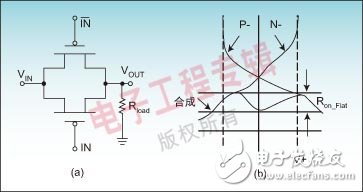
Figure 1a is a simplified schematic diagram of an analog switch. It can be seen from the figure that the normally open normally closed channel of an analog switch is actually composed of two dual N-channel MOSFETs and a P-channel MOSFET, which can transmit signals bidirectionally. The P-channel MOSFET corresponding to different VIN values ​​is connected in parallel with the on-resistance of the N-channel MOSFET, and the relationship between Ron and the input voltage (VIN) in the parallel structure of FIG. 1b can be obtained. If the influence of temperature and power supply voltage is not considered, Ron A linear relationship with Vin will cause a change in insertion loss, causing the analog switch to produce total harmonic distortion (THD). In addition, Ron is also affected by the power supply voltage and usually decreases as the power supply voltage rises.

Figure 1: a. Analog switch schematic; b. Analog switch on-resistance versus input voltage
2. The analog switch input has a strict input signal range
Since the analog switch is a semiconductor device, when the input signal is too low (below zero potential) or too high (higher than the supply voltage), the MOSFET is reverse biased when the voltage reaches a certain value (exceeding the limit of 0.3V) At this time, the switch can not work normally, and even severely damaged. Therefore, in the application of analog switches, it must be noted that the input signal should not exceed the specified range.
3. Injecting charge
Applying mechanical switches We certainly hope that the lower the Ron, the better, because low resistance can reduce signal loss. However, for analog switches, low Ron is not suitable for all applications. Lower Ron needs to occupy a larger chip area, resulting in a larger input capacitance, which consumes more charge and discharge during each switching cycle. Current. The time constant t = RC, the charging time depends on the load resistance (R) and capacitance (C), generally lasting for tens of nanoseconds. This shows that low Ron has longer turn-on and turn-off times. To this end, the choice of analog switches should be a trade-off between Ron and injected charge.
4. There will still be an inductive signal leakage when the switch is turned off.
This feature means that when the analog switch transmits an AC signal, in the case of a disconnection, a part of the signal is still transmitted from the input to the output through induction, or from one channel to the other. Usually the higher the frequency of the signal, the more severe the signal leakage.
5. The transmission current is relatively small
Analog switches are different from mechanical switches. They usually only transmit small currents. Currently, analog switches in CMOS technology allow continuous currents to be mostly less than 500 mA.
6. Logic control terminal drive current is very small
The drive current of the mechanical switch logic control terminal is often milliampere, and sometimes it is difficult to drive by digital I/O alone. The logic control terminal of the analog switch has a very small driving current, which is generally lower than the nanoampere level. Therefore, it can be directly driven by digital I/O, thereby reducing power consumption and simplifying the circuit.
Analog switch switching characteristics
Since it is called an analog switch, it is naturally also switchable, as follows:
1. Signal can be transmitted in both directions
Some people are accustomed to calling the two normally open and closed ends of the analog switch as the input, and the common terminal is called the output. In fact, this is only a temporary definition based on the specific application of the analog switch. Most of the analog switches can make the signals transmit in both directions. If you ignore this, it is easy to make the circuit generate problems, such as reverse voltage bias, current backflow, and so on.
2. The leakage current is very small after the switch is turned off
The analog switch will exhibit a high-impedance state when it is OFF. The leakage current between the two transmission terminals is extremely small. Generally, it is only below the nanoampere level. For example, the SGM3001, SGM3002, and SGM3005 series analog switches have leakage currents after disconnection. It is 1nA. Such a weak current is negligible in the application, and the analog switch can now be considered to be ideally disconnected.
In short, the analog switch is a semiconductor device with a switching function. In the application process, it is necessary to make full use of its switching function and its semiconductor characteristics, otherwise unexpected trouble may occur.
Analog switch application example analysis
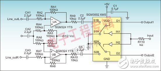
2 is a front-end amplification and signal gating circuit of an audio device, in which SGM324 (four-channel operational amplifier) ​​and SGM3002 (dual-channel analog switch) are selected.

Figure 2: Audio front end amplification and signal strobe circuit
The design of the scheme is intended to be that when Input=0, the Line_outL and Line_outR audio signals are strobed; when Input=1, the Phone_outL and Phone_outR audio signals are strobed. However, when the experimental machine was made, the designer found that when Input=1, a considerable part of the Line_outL and Line_outR channels leaked to the D1 and D2 terminals respectively. Using the network analyzer HP/Agilent 3589A to test the turn-off isolation of the SGM3002, when the input signal is 10kHz, the turn-off isolation of the SGM3002 is only -120dB, so the chip should be no problem.
In fact, the circuit has the following two errors in the analog switch application:
1. The analog input signal lacks a DC offset
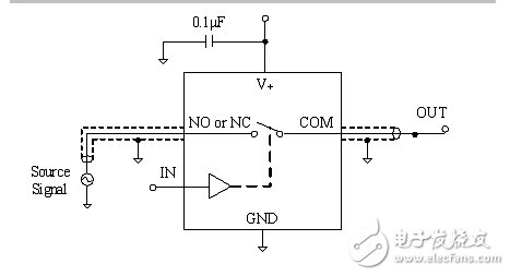
The analog switch portion of the circuit in Figure 2 can be equivalent to Figure 3. The first part of this article has mentioned that the analog switch input signal input cannot be negative.

Figure 3: Analog Switch Equivalent Circuit
Generally speaking, the analog switch input signal of the CMOS process can only be as small as -0.3V. If it is lower than this value, the chip will not work normally or even be damaged. In Figure 2, the analog switch input signal has no DC offset, so some of the input signal is in the negative zone, and the analog switch naturally does not work properly.
Solution: Remove the capacitors C2 and C3, and the analog switch input signal will have a 1/2 VDC bias signal. At this time, the analog switch can work in rail-to-rail mode. In addition, since the capacitor is added to the common side of the analog switch, the DC signal can still be effectively isolated.
2. Missing Coupling resistor at terminals D1 and D2
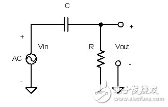
When the analog switch is open, its input and output are equivalently connected in series with a capacitor C. If it is assumed that there is an equivalent resistance R between the analog switch output and ground, the analog switch is disconnected. The equivalent circuit is shown in Figure 4.

Figure 4: Equivalent circuit when the analog switch is turned off
The analog switch at this time is equivalent to an RC filter circuit, so it is not difficult to get the following formula:

Among them, uout is the analog switch output signal; uin is the analog switch input signal; R is the analog switch output resistance load; C is the equivalent capacitance when the analog switch is off; f is the input signal frequency.
Since the analog switch equivalent capacitance C is designed to be small, when the input signal f is in the audio zone, the gain A is determined by both R and f. When R is small, f plays a leading role. At this time, A "1, the signal is effectively isolated. When R takes a large value, R plays a leading role at this time. At this time, A—“1, the signal is almost completely leaked. Therefore, when the output terminal is suspended, the resistance R-"+∞ between the output terminal and the ground is complete, and the analog switch is fully turned on.
After correcting the above two errors, the audio application circuit can work normally. As can be seen from the above examples, a thorough understanding of the basic concept of an analog switch is the basis for the correct application of an analog switch.
Modern Physics Experiment Series
Modern physics experiment related equipment for efficient specialized physics laboratory
Modern Physics Experiment Instruments,Optical Instruments,Acousto-Optic Modulator Experimental Device,Optical Spectroscopy Experiment Determinator
Yuheng Optics Co., Ltd.(Changchun) , https://www.yhenoptics.com