Increased performance means that designers can achieve higher data throughput for faster image acquisition, use higher resolution sensors, and take full advantage of some of the newest cameras on the market with the highest dynamic range. The increase in performance not only allows designers to capture images faster but also processes images more quickly. Preprocessing algorithms (such as thresholding and filtering) or processing algorithms (such as pattern matching) can also be performed more quickly. Ultimately, designers can make decisions based on visual data faster than ever before.
As vision systems increasingly incorporate the latest generation of multi-core CPUs and powerful FPGAs, vision system designers need to understand the benefits and success of using these processing elements. Not only do they need to run the right algorithms on the right hardware, they also need to understand which architectures are best suited to their design.
Inline processing and co-processing
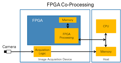
Before studying which type of algorithm is best for which processing element, you should understand the most appropriate architecture type for each application. When developing a vision system based on a heterogeneous architecture of CPUs and FPGAs, two major usage scenarios need to be considered: embedded processing and co-processing. If it is FPGA co-processing, FPGA and CPU will work together to share processing load. This architecture is most commonly used for GigE Vision and USB3 Vision cameras because their acquisition logic is best implemented on the CPU. You can use the CPU to capture the image and then send it to the FPGA via direct memory access (DMA) so that the FPGA can perform operations such as filtering or color plane extraction. You can then send the image back to the CPU for more advanced operations such as optical character recognition (OCR) or pattern matching. In some cases, you can implement all the processing steps on the FPGA and send only the processing results back to the CPU. This allows the CPU to use more resources for other operations such as motion control, network communication, and image display.

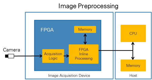
In the embedded FPGA processing architecture, you can connect the camera interface directly to the pins of the FPGA so that pixels can be sent directly from the camera to the FPGA. This architecture is often used with Camera Link cameras because their acquisition logic is easily implemented using digital circuitry on the FPGA. There are two main benefits to this architecture. First, as with coprocessing, embedded processing can be used to transfer part of the work from the CPU to the FPGA when performing preprocessing on the FPGA. For example, high-speed preprocessing such as filtering or thresholding can be performed on the FPGA before sending the pixels to the CPU. This also reduces the amount of data the CPU must process because the logic on the CPU only needs to capture the pixels of the region of interest, which ultimately increases the overall system throughput. The second benefit of this architecture is the ability to perform high-speed control operations directly within the FPGA without using the CPU. FPGAs are ideal for control applications because they can provide very fast and highly deterministic loop rates. One example is high-speed classification, where the FPGA sends pulses to the actuator, and the actuator rejects or categorizes the part as it passes through the actuator.

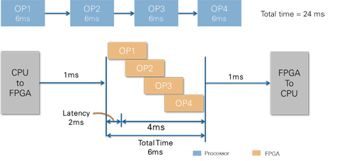
CPU and FPGA vision algorithms <br> Having a basic understanding of the different ways of building heterogeneous vision systems, you can look at the best algorithms that run on FPGAs. The first thing to understand is how the CPU and FPGA work. To explain this concept, we assume that a theoretical algorithm can perform four different operations on an image, and then look at how these four operations operate when deployed on a CPU and an FPGA, respectively.
The CPU executes the operations in sequence, so the first operation must be completed after the entire image has finished running before the second operation can be started. In this example, assume that each step in the algorithm takes 6ms to run on the CPU; therefore, the total processing time is 24 milliseconds. Now consider running the same algorithm on the FPGA. Since FPGAs are essentially massively parallel, the four operations in this algorithm can operate on different pixels in the image at the same time. This means that it takes only 2 ms to receive the first processed pixel and 4 ms to process the entire image, and therefore the total processing time is 6 ms. This is much faster than the CPU. Even if an FPGA is used to co-process the architecture and transfer images to the CPU, the overall processing time (including transfer time) is much shorter than if the CPU were used alone.

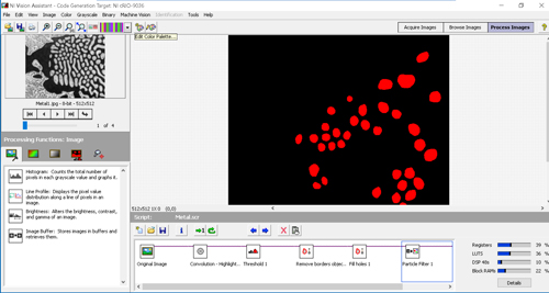
Now consider a real example, such as the image required for particle counting. You first need to apply a convolution filter to sharpen the image. Next, the image is run through a threshold to generate a binary image. This can not only reduce the amount of data in the image by converting it from 8-bit monochrome to binary, but also prepare images for binary morphology applications. The final step is to use morphology to apply the shutdown feature. This will remove any holes in the binary particles.
If the above algorithm is only executed on the CPU, the convolution step of the entire image must be completed before the threshold step starts. When using the Vision Development Module for LabVIEW from National Instruments and the cRIO-9068 CompactRIO controller based on the Xilinx Zynq-7020 All Programmable SoC, the time required to execute the above algorithm is 166.7 ms. However, if you run the same algorithm on an FPGA, each step can be performed in parallel. Running the same algorithm on the FPGA takes only 8ms to complete. Remember that the 8ms time includes the DMA transfer time from sending the image from the CPU to the FPGA, and the time the algorithm was completed. In some applications, the processed image may need to be sent back to the CPU for use by other parts of the supply. If you add this time, the entire process is only 8.5ms. In general, the FPGA executes this algorithm 20 times faster than the CPU.

So why not run each algorithm on the FPGA? Although FPGAs are more beneficial to visual processing than CPUs, there are certain tradeoffs to enjoying these advantages. For example, consider the original clock frequency of the CPU and FPGA. The FPGA clock frequency is in the order of 100 to 200 MHz. Obviously, the FPGA clock frequency is lower than the CPU clock frequency, and the CPU can easily run at 3GHz or higher. Therefore, if an application requires an image processing algorithm that must be run iteratively and cannot take advantage of the parallelism of the FPGA, then the CPU can process it faster. The example algorithm discussed earlier runs on the FPGA to achieve a 20x speed increase. Each processing step in the algorithm operates on each pixel or set of pixels at the same time, so the algorithm can use the parallel advantages of FPGA to process images. However, if the algorithm uses processing steps such as pattern matching and OCR, these requirements immediately analyze the entire image, and the advantages of FPGA are far less advantageous. This is due to the lack of parallelization of the processing steps and the large amount of memory needed to perform the alignment analysis between images and templates. Although FPGAs have direct access to internal and external memory, in general, the amount of memory available to the FPGA is far less than the number of CPUs available or the number of these processing operations.
Overcome programming complexity
The advantages of FPGAs for image processing depend on each application requirement, including application-specific algorithms, delay or jitter requirements, I/O synchronization, and power consumption. Commonly used architectures with FPGAs and CPUs can take full advantage of the respective advantages of FPGAs and CPUs and have competitive advantages in performance, cost, and reliability. However, one of the biggest challenges in implementing FPGA-based vision systems is to overcome the FPGA's programming complexity. Visual algorithm development is essentially an iterative process. You must try a variety of methods to complete any task. In most cases, what needs to be determined is not which method is feasible, but which method is best, and the "best method" decision is different for different applications. For example, speed is important for some applications, and accuracy is more important for other applications. At the very least, you need to try several different ways to find the best method for a particular application.
In order to maximize productivity, no matter which processing platform is used, feedback on the algorithm and benchmarking information are needed immediately. When using iterative exploratory methods, real-time viewing of algorithm results will save a lot of time. What is the correct threshold? How big or small are the particles removed by the binary form filter? Which image preprocessing algorithm and algorithm parameters can best clean the image? These are common problems when developing visual algorithms, but the key lies in whether you can change and quickly see the results. However, traditional FPGA development methods may slow innovation because compile time is required between each design change of the algorithm. One way to overcome this is to use an algorithm development tool that allows you to perform CPU and FPGA development in the same environment without complicating the FPGA. NI Vision Assistant is an algorithm engineering tool for developing algorithms deployed on CPUs or FPGAs to help you simplify visual system design. You can also use Vision Assistant to compile and run pre-test algorithms on target hardware while easily accessing throughput and resource utilization information.

So when considering who is more suitable for image processing, CPU or FPGA? The answer is "depending on the circumstances." You need to understand the application's goals in order to use the processing element that best fits the design. However, regardless of the application, CPU-based or FPGA-based architectures and their inherent advantages can increase the performance of machine vision applications by one level.
Strain/flex Reliefs And Grommets
the power Connectors we provide overmolding solutions and modular tooling.
We also offer to the OEM and distributor users a diversified line of strain / flex reliefs and grommets, such as Solid, Solid-Rib, Uniflex, Multiflex, in standard off the shelf or custom designs.
Overmolding the power connectors offers significant opportunities for cable improvements with higher pull strength not available with conventional backshells. Our technical staff is ready to help you from design and prototyping to small production run, assistance, and training.
Our team is ready to help with any of the following power connectors projects: overmolding mini fit jr. and mini-fit sr. connectors, , overmolded cables with micro fit terminations, sabre molded cable asemblies, amp duac overmolded power connectors, mate-n-lock power cables, power connector overmolding services, power connector molding, design and prototype of power cables across the board, small run molded power connecotrs , molded cable manufacturing, overmolding connectors for any power applications
Strain Reliefs And Grommets,Flex Reliefs And Grommets,Cable Strain Reliefs,Cable Flex Reliefs,Cable Grommets,Molded Strain Relief
ETOP WIREHARNESS LIMITED , https://www.oemmoldedcables.com