Abstract: Explain in detail the problems that should be paid attention to when designing high-speed digital printed circuit boards, and clarify the impact of high-speed digital circuits on train in-vehicle systems, and the reasons for these effects. There are several ways you should take the circuit. Practice has proved that the circuit designed by these methods can greatly improve the anti-jamming performance of the product.
This article refers to the address: http://
1 Introduction
With the continuous development of science and technology, the train is also developing at a high speed, and high-speed digital circuits are gradually adopted in the train vehicle system. There are many sources of interference on the train, including electromagnetic interference generated by various types of transformers, fans, pantographs, air compressors, etc., which affects the normal operation of high-speed digital circuits in trains. In addition, in order to ensure the comfort of the riding environment and the working environment, the car is also equipped with various electrical appliances such as air conditioners, electric heaters, ventilators, etc. They also generate electromagnetic radiation externally, which affects the normal operation of high-speed digital circuits. Therefore, in such a complex environment on the train, how to ensure the reliability of high-speed digital signals will become more and more important. If these problems are not handled well, it will lead to signal distortion, timing errors, system instability and many other situations, which will bring unpredictable losses.
In order to ensure the normal operation of the train communication, control and other systems, the anti-interference design and functional design of the equipment are equally important. At the beginning of the design, the suppression of digital circuit interference must be considered. Otherwise, it is difficult to meet the anti-interference requirements of high-speed digital circuits. Therefore, it is first necessary to improve the anti-interference ability of the digital circuit board and reduce the circuit radiation, so as to avoid the remedial measures against the interference of the circuit board after the design is completed.
2 interference formation method
The three basic ways of interference formation: interference sources, coupling paths, and sensitive sources. The following are explained from these aspects.
2.1 PCB circuit board interference coupling approach
Interference on the PCB board mainly includes common mode interference and differential mode interference. Differential mode interference is generated by the signal loop, which is generated by the common mode current on the cable. For a printed circuit board, it mainly refers to its differential mode interference, because the frequency range of differential mode interference is the entire frequency band occupied by the circuit signal, not only can it be coupled to each sensitive source device through its wire, but also the current ring is coupled into the external generation. Various types of interference affect the normal working system. The main method to reduce differential mode interference is to minimize the length of the trace and reduce the signal loop area during wiring.
2.2 Interference source generation method on PCB circuit board
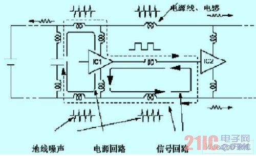
The main cause of various types of interference in high-speed digital circuits is the inherent noise frequency of the power supply and the di/dt and du/dt of various changes on the external line. Because of the existence of power supply circuits, signal circuits, high-speed signal circuits and accessories on the circuit board. All kinds of capacitive and inductive loads on the line, so when the signal is hopped, a spike will be generated to form noise, and these noises will be transmitted along the current loop of each loop. Therefore, the inherent noise of the power supply itself should be suppressed. A kind of noise caused by high-speed digital hopping. To suppress the noise generated by the circuit itself or various types of abrupt signals, the best way to suppress is decoupling and filtering. This not only reduces its own noise but also absorbs external influences and improves its anti-interference ability. Figure 1 briefly illustrates the noise generated during each circuit phase.

Figure 1 Noise generation in each circuit stage
2.3 Sensitive sources on the PCB board
For high-speed digital signal sensitive sources mainly refer to objects that are susceptible to external interference, such as: A / D, D / A converter, logic controller, microcontroller, crystal oscillator, digital IC, weak signal amplifier. The stability of these devices is directly related to the stability and working accuracy of the system operation of the board. Therefore, these sensitive sources should be properly protected to improve their anti-interference ability.
3 Improve PCB circuit board anti-interference measures
3.1 Reduce the coupling loop
The main method to reduce the coupling is to reduce the signal loop area, which should mainly solve the loop area of ​​the ground wire, power supply, sensitive signal source and board edge.
3.1.1 Reduce grounding and power coupling loop
Ground impedance is the main cause of ground noise on the board. Therefore, the ground line impedance should be minimized. Ground plane or grid ground can be used.
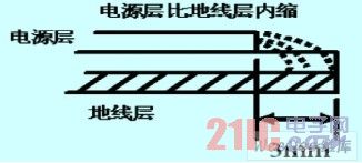
For high-speed digital circuit boards, multi-layer boards should be used to reduce the loop area. The middle layer should be used as the power source or ground plane, and the spacing between the power supply and the ground should be as small as possible; let each signal layer have a corresponding ground. In the line layer, the ring area formed by the signal line and its ground loop should be as small as possible, and the smaller the ring area, the less external interference. In view of this feature, in the ground plane segmentation, the distribution of the ground plane and important signal traces should be taken into consideration to prevent problems caused by the ground plane slotting, etc. The signal lines cannot cross the ground plane and the power plane separation area to prevent formation. Large ground loop. At the same time, the power plane should be reduced by about 3 mm from the ground plane, which will suppress more than 70% of power supply interference. as shown in picture 2.

Figure 2 Schematic diagram of the power layer than the ground layer
3.1.2 Coupling loop for reducing sensitive source signals
For sensitive signals such as: periodic signals, such as clock signals, analog signals, low-level signals of the address bus, etc., the interference is strong, which is also the key to design high-speed digital circuits. The key signal wiring on the printed board should be routed from high to low (sorting method: high to low: analog signal - reset signal - I2C - clock signal - read / write signal - high speed, RF signal - data bus - address bus ); the key signal wiring should go as far as possible to the inner layer; and it should be matched with small capacitors for parallel filtering; the signal layer can only be paralleled by two layers after ground plane isolation; the signal line should be as short as possible; The components of the high-frequency wiring on the printed board are as short as possible to the trace; to reduce the distribution parameters and electromagnetic interference of the high-frequency signal, so as to improve the anti-interference ability of the sensitive signal source.
3.1.3 Reducing the coupling loop at the edge of the board
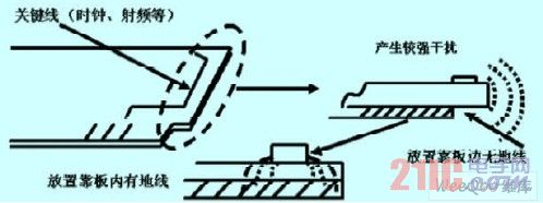
Whether the board edge processing of the printed circuit board is reasonable determines whether the external interference of the signal can be more effectively suppressed. In order to prevent high-speed digital circuits from interfering with the board edge, the wiring position should be strictly controlled so that it is as close as possible to the inside of the printed board. High-frequency interference, strong signal lines should not go to the edge of the board to prevent the corresponding layer coupling loop, resulting in external interference leakage, as shown in Figure 3:

Figure 3 The coupling loop on the side of the board
3.2 Suppression of interference sources
The suppression of interference sources is to minimize the effects of interference sources du/dt and di/dt. Reducing the interference source du/dt is mainly achieved by paralleling the capacitance across the interference source, increasing decoupling and filtering. Reducing the interference source di/dt is mainly achieved by series inductance in the interference source or by adding a freewheeling diode. For example, adding a freewheeling diode to the relay can eliminate the back EMF interference generated when the coil is disconnected.
3.2.1 Increase the decoupling capacitor
The decoupling capacitor is the filtering object of the output signal. The addition of parallel decoupling capacitors on the chip eliminates the effects of self-excitation and suppression of level changes, allowing the power supply noise and level changes to flow back to ground with the shortest path, increasing the immunity to interference. In order to suppress the noise well, each chip should be equipped with a decoupling capacitor as much as possible, and the decoupling capacitor should be placed as close as possible to the chip power supply and the ground pin. The decoupling capacitor is generally 0.01-0.1 uf, which can be taken as C=1/F, 0.1 uf for 10 MHZ and 0.01 uf for 100 MHz. The higher the frequency, the smaller the decoupling capacitor should be.
3.2.2 Circuit Filter Absorption
For the abrupt signal that is prone to burrs, the corresponding filtering form should be adopted to suppress the high frequency glitch generated by the mutation of the high speed signal. The filtering method generally uses a passive component capacitor or an inductor to match the resistor, and uses the energy storage characteristics of the voltage and current to achieve the filtering purpose. The RC filter circuit is often used. When the voltage suddenly rises, the parallel capacitor C can store energy, and when the voltage drops, the energy is released, so that the voltage after the load is filtered is smoother and the high frequency noise is reduced. However, in order not to affect the normal high-frequency signal waveform, the value cannot be too large, so try to use a small capacitor. According to the total impedance of the circuit and the bandwidth and rise time of the high-frequency signal, according to the calculation and experience, the selection of the filter capacitor C is as follows: Refer to the following table 1: The higher the system operating frequency, the smaller the filter capacitor should be.
Table 1 Selection of Filter Capacitor in Various Cases

4 Conclusion
The reliability of the anti-jamming design of high-speed digital circuits has a profound impact on the overall performance of the entire electronic and electrical equipment. The reliability of any product should be taken from the source of the design. Only by knowing the reliability design of the printed circuit can the product be guaranteed. Reliability, truly improve the reliability of printed boards.
Through various types of diagrams, it can be seen that the high-speed digital printed circuit board improved according to the method can reduce the noise generated by itself and improve its anti-interference ability. From the economic considerations of R&D costs, considering the anti-interference problem of the circuit at the beginning of the design will save a lot of repetitive design costs. This method has achieved good practical results in the internal promotion of Times Electric Company's technology center, and improved the one-time success probability of the board, which not only saves design cost but also improves design efficiency.
1.ANTENK Wire to Board connectors are avialable in different terminations and sizes intended for use on a variety of applications. These connectors provide power and signal with different body styles, termination options, and centerlines. To find the wire to board set required, click on the appropriate sub section below.
2.Our products are widely used in electronic equipments,such as monitors ,electronic instruments,computer motherboards,program-controlled switchboards,LED,digital cameras,MP4 players,a variety of removable storage disks,cordless telephones,walkie-talkies,mobile phones,digital home appliances and electronic toys,high-speed train,aviation,communication station,Military and so on
Antenk Wire To Board Connectors Ranges:
Power Wire to Board
IDC Wire to Board
Locking Wire to Board
Latching Wire to Board
Fine Pitch Wire to Board
Wire to Board Connectors Information
Description
Wire-to-board connectors are used to interconnect printed circuit boards (PCBs) by using connectors attached to wires.
Specifications
Specifications for a wire to board connector include the following.
Wire-entry angle - There are three wire-entry angle styles: vertical, right-angle, and bottom-entry.
Wire size - Wire size is usually measured in American wire gauge (AWG), a standard for non-ferrous wire conductor sizes. The term "gauge" refers to the wire`s diameter. The higher the gauge number, the smaller the diameter and the thinner the wire.
Circuits or positions - With wire to board connectors, the number of circuits or positions may range from 1 to 120.
Pitch or center spacing - Pitch or center spacing is measured in millimeters (mm) or inches.
Lock to mating style - There are three basic lock-to-mating styles: positive, friction, and friction ramp.
Maximum current - The maximum current or current-carrying capacity is measured in amperes (A) and ranges from 1.0 A to 50. A.
Termination Methods
Crimp is the physical compression of a contact wire around a conductor to make an electrical and mechanical connection. Insulation displacement connectors (IDC) slice through the cable insulation to make a connection. Choices for termination method also include cage clamp, screw, tabs, and solder cups.
PCB Mounting Styles
With wire to board connectors, there are four choices for PCB mounting.
Through-hole technology (THT) mounts components on a PCB by inserting component leads through holes in the board and then soldering the leads in place on the opposite side of the board.
Surface mount technology (SMT) adds components to a PCB by soldering component leads or terminals to the top surface of the board. SMT components have a flat surface that is soldered to a flat pad on the face of the PCB. Typically, the PCB pad is coated with a paste-like formulation of solder and flux.
Press-fit and compression-style Board To Board Connectors are also commonly available.Wire to Board Connectors Information
Standards
Wire-to-board connectors carry approvals from various national and international organizations. In North America, they often bear marks from Underwriters Laboratories (UL) and/or the Canadian Standards Association (CSA).
A wire to board connector for the European marketplace should comply with the Restriction of Hazardous Substances (RoHS) and Waste Electrical and Electronic Equipment (WEEE) directives from the European Union (EU). Wire-to-board connectors that comply with other requirements are also available.
BS 9526 N0001 - Specification for multi-contact edge socket electrical connectors.
Wire To Board Connectors,Wire Harness,Pcb Wire To Board Connector,Pin Wire To Board Connector,IDC Wire to Board,Locking Wire to Board,Latching Wire to Board,Fine Pitch Wire to Board
ShenZhen Antenk Electronics Co,Ltd , https://www.antenk.com