Guide: When you buy a camera, you will usually see a COMS lens and a CCD lens. What is the difference between these two lenses? What are their characteristics? Let us look at their self-introduction.

The difference between cmos and ccd - CCD introduction
The full name of CCD in English is "Charge-coupledDevice", the full name of Chinese is electric line coupling element, usually called CCD image sensor. CCD is a kind of semiconductor device that can convert optical images into digital signals. The tiny photosensitive substances implanted on the CCD are called pixels. The more pixels contained in a CCO, the more the resolution of the screen is. high. The CCD acts like a film, but it converts the image pixels into digital signals. The CCD has a number of neatly arranged capacitors that sense light and convert the image into a digital signal. Through the control of the external circuit, each small capacitor can transfer its electric current to its adjacent capacitor.
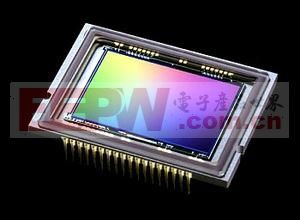
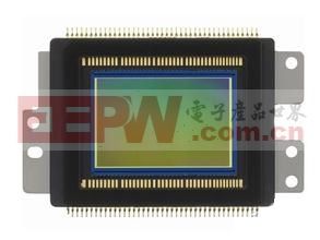
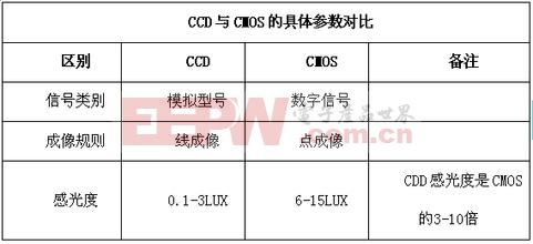
The CCD image sensor can directly convert the optical signal into an analog current signal. The current signal is amplified and analog-digital converted to achieve image acquisition, storage, transmission, processing and reproduction. As shown in the above figure, the CCO image sensor has the following characteristics:
(1) small size and light weight
(2) Low power consumption, low working voltage; anti-impact and vibration, stable performance and long life
(3) High sensitivity, low noise, and large dynamic range
(4) fast response, self-scanning function, small image distortion, no afterimage
(5) Application of VLSI process technology, high pixel integration, accurate size, and low commercial production cost.
The difference between cmos and ccd - Introduction to COMS
CMOS (Compementary Metal Oxide Semiconductor) refers to a complementary metal oxide semiconductor, which is an amplifier component of voltage control and is a basic unit constituting a CMOS digital integrated circuit. In the field of digital imaging, CMOS has been developed as a low-cost photosensitive element technology. The common digital products on the market are mainly CCD or CMOS, especially low-end camera products, and usually high-end cameras are CCD-sensitive. element.
The CMOS manufacturing process is applied to the photosensitive element of digital image equipment. It converts the function of pure logic operation into the external light and converts it into electric energy. The image signal converted by the analog-to-digital converter (ADC) on the chip is transformed. Output for digital signals. CMOS and CCD mainly have the following differences:
(1) High noise generated during imaging
(2) High integration
(3) The reading speed is fast, the address strobe switch can be randomly sampled to obtain higher speed
(4) Noise: Due to the high integration of CMOS image sensors, the distance between components and circuits is very close, the interference is serious, and noise has a great influence on image quality. With the continuous development of CMOS circuit noise reduction technology, it provides good conditions for producing high-density and high-quality CMOS image sensors.
The difference between cmos and ccd - technical comparison
1) Information reading method
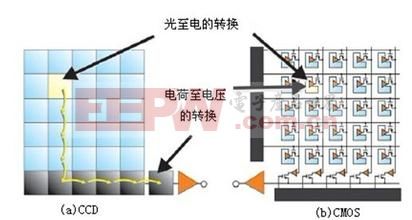
The charge information stored by the CCD charge coupler needs to be read one bit after the synchronization signal control. The charge information transfer and the read output need to have a clock control circuit and three different sets of power supplies. The whole circuit is more complex. The CMOS photoelectric sensor directly generates a current (or voltage) signal after photoelectric conversion, and the signal reading is very simple.
2) Speed
The CCD charge coupler needs to output information one bit at a time in the behavior unit under the control of the synchronous clock, and the speed is slow; while the CMOS photoelectric sensor can extract the electric signal and simultaneously process the image of each unit. Information, speed is much faster than CCD charge couplers.
3) Power and power consumption
CCD charge couplers mostly need three sets of Power Supply, which consumes a lot of power; CMOS photoelectric sensors only need to use one power supply, and the power consumption is very small, only 1/8 to 1/10 of CCD charge coupler, CMOS photoelectric sensor It has great advantages in energy saving.
4) Image quality
CCD charge coupler fabrication technology started early, the technology is mature, and the noise is isolated by PN junction or silicon dioxide (SiO2) isolation layer. The imaging quality has certain advantages over CMOS photoelectric sensors. Due to the high integration of CMOS photoelectric sensors, the distance between each photoelectric sensing element and circuit is very close, and the optical, electrical and magnetic interference between them is serious. The noise has a great influence on the image quality, making the CMOS photoelectric sensor for a long time. Unable to enter practical. In recent years, with the continuous development of CMOS circuit noise reduction technology, it has provided good conditions for the production of high-density and high-quality CMOS image sensors.
The difference between cmos and ccd - structural differences
1. Internal structure (structure of the sensor itself)
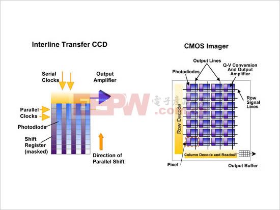
The imaging points of the CCD are arranged in an XY vertical and horizontal matrix, each imaging point consisting of a photodiode and an adjacent charge storage area controlled by it. Photodiodes convert light (photons) into electric charges (electrons), and the amount of electrons collected is proportional to the intensity of the light. When these charges are read, each row of data is moved to a buffer in the direction of vertical charge transfer. The charge information for each row is continuously read and sensed by the charge/voltage converter and amplifier. The image produced by this configuration has the characteristics of low noise and high performance. However, the production of CCD requires a clock signal and a bias voltage technology, so the overall structure is complicated, which increases power consumption and increases cost.
Electronics around the CMOS sensor, such as digital logic, clock drivers, and analog-to-digital converters, can be integrated in the same processing program. The CMOS sensor is constructed like a memory, each imaging point contains a photodiode, a charge/voltage conversion unit, a reset and selection transistor, and an amplifier covering the entire sensor with a metal interconnect (chrono application and Read signals) and longitudinally arranged output signal interconnects that can read signals with simple XY addressing techniques.
2. External structure (application structure of the sensor on the product)
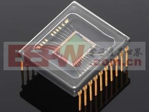
The CCD charge coupler needs to output information one bit at a time in the behavior unit under the control of the synchronous clock, and the speed is slow; while the CMOS photoelectric sensor can extract the electric signal and simultaneously process the image of each unit. Information, speed is much faster than CCD charge couplers.
The processing of CMOS photoelectric sensors uses the process of semiconductor manufacturers to produce integrated circuits, which can integrate all components of digital cameras onto a single chip, such as photosensitive elements, image signal amplifiers, signal reading circuits, analog-to-digital converters, image signal processors, and Controllers, etc., can be integrated into one chip and have the advantage of additional DRAM. A lot of functions can be realized with only one chip, so the overall cost of the photoelectric image conversion system using the CMOS chip is low.
The main difference between CCD and CMOS in manufacturing is that CCD is integrated on semiconductor single crystal material, and CMOS is integrated on semiconductor material called metal oxide. There is no essential difference in working principle. CCD only has a few manufacturers such as Sony and Panasonic to master this technology. Moreover, the CCD manufacturing process is more complicated, and the price of the camera using the CCD is relatively expensive. In fact, after the technical transformation, the gap between the actual effects of CCD and CMOS has been reduced a lot. Moreover, the manufacturing cost and power consumption of CMOS are lower than that of CCD, so many CMOS sensors used by camera manufacturers. Imaging: The imaging transparency and sharpness of the CCD are very good under the same pixel, and the color reproduction and exposure can be basically accurate. The CMOS products are generally transparent, the color reproduction ability of the real object is weak, and the exposure is not very good. Due to its physical characteristics, the imaging quality of the CMOS and the CCD still have a certain distance. However, due to its low price and high integration, it has been widely used in the field of cameras.
The difference between cmos and ccd - summary
The CMOS structure is relatively simple, and is the same as the existing large-scale integrated circuit production process, so that the production cost can be reduced. In principle, the CMOS signal is a charge signal in points, and the CCD is a current signal in the unit of action. The former is more sensitive, the speed is faster, and the power is saved. Now advanced CMOS is not worse than the general CCD, but the CMOS process is not very mature. Ordinary CMOS generally has low resolution and poor imaging.
The current situation is that many low-end entry-level digital cameras use inexpensive low-end CMOS chips, and the image quality is poor. Popular, advanced and professional digital cameras use different grades of CCDs, and individual professional or quasi-professional digital cameras use advanced CMOS chips. The X3 chip, which represents the future development of imaging technology, is actually a CMOS chip. CCD and CMOS are not good or bad, but in general, the quality of imaging using CCD chips in popular digital cameras is better.
It can be seen from the working principle of two kinds of photosensitive devices that CCD (Charge Coupled Device) has the advantage that the image quality is good, but due to the complicated manufacturing process, only a few manufacturers can master it, thus leading to manufacturing. The cost is high, especially for large CCDs, which are very expensive. At the same resolution, CMOS (Complementary Metal-Oxide Semiconductor) is cheaper than CCD, but the image quality produced by CMOS devices is lower than that of CCD. So far, the vast majority of consumer grades and high-end digital cameras on the market use CCD as a sensor; CMOS sensors are used as low-end products on some cameras, if any camera manufacturer produces a camera using a CCD sensor Manufacturers will spare no effort to promote it as a selling point, even under the name of "digital camera." For a time, whether or not there is a CCD sensor has become one of the standards for people to judge the grade of digital cameras.
The main advantage of CMOS for CCD is that it is very power-saving. Unlike CCDs made up of diodes, CMOS circuits have almost no static power consumption, and only when the circuit is turned on, there is power consumption. This makes the power consumption of CMOS only about 1/3 of that of ordinary CCD, which helps to improve the bad impression that digital cameras are "electric tigers". The main problem with CMOS is that when dealing with fast-changing images, the current changes too often and overheats. If the dark current is suppressed well, the problem is not big. If the suppression is not good, the noise is very likely to occur.
In addition, CMOS and CCD image data scanning methods are very different. For example, if the resolution is 3 megapixels, the CCD sensor can continuously scan 3 million charges. The scanning method is very simple, as if the bucket was passed from one person to another, and only after the last data scan was completed. Amplify the signal. Each pixel of a CMOS sensor has an amplifier that converts the charge into an electrical signal. Therefore, the CMOS sensor can perform signal amplification on a per-pixel basis. This method can save any invalid transmission operation, so fast data scanning can be performed with a small amount of energy consumption, and noise is also reduced. This is Canon's in-pixel charge transfer technology.
Thyristor
Speech Translation Mouse,Speech Input Mouse,Voice Search Mouse,Sound Receiver Mouse
Guangzhou Lufeng Electronic Technology Co. , Ltd. , https://www.lufengelectronics.com
