Recently, innovations in portable wearable medical devices have greatly facilitated the need to minimize the size of semiconductor components. Many of these devices require on-board memory to store calibration data, test results, and data logs. A common solution is to use non-volatile memory products such as serial EEPROM or flash memory that meet the high reliability and low power requirements of portable medical applications. Wearable medical devices are usually designed to be as concealed as possible. Therefore, it is necessary to achieve the required storage density in a package as small as possible. For example, the customizability of hearing aids is increasing, programming for specific users, providing multiple modes for different auditory environments, and providing data logs for further adjustments in subsequent arrangements. These innovations require more data to be stored in a limited form factor. To meet this, many medical device designers are turning to innovative die memory solutions.

Although die is the smallest form of storage device, it faces significant challenges in processing, storage, and assembly. The traditional way to use die is to order a single wafer from a semiconductor supplier. However, this requires medical device manufacturers to seek solutions for wafer and bonded wafers. For some manufacturers, this is beyond their capabilities. While these services can be outsourced, an alternative solution is to purchase "in-frame wafers" - some kind of cut wafer. The cut wafer is placed in an adhesive film supported by a metal frame. By ordering such wafers, medical device manufacturers will receive small pieces of die for sorting and placement.
The next challenge is how to electrically connect the die to the application. The traditional approach is to cure the die on the board with epoxy and then wire the leads to electrically connect the die. The die is then packaged in a protective epoxy housing. This is not a simple matter, because of the high requirements for the placement accuracy of the die, special equipment is required. An alternative is to use a bumped die. Such a die has metallized its pads and fixed the pads to the pads. Reflow soldering can be used to connect the bumped die directly down the PCB. Due to the different thermal expansion (CTE) coefficients of the silicon die and the PCB, the bumped die presents a risk of solder joint shear strain. For this reason, bumped dies are typically filled with additional adhesive at the bottom to provide a stronger mechanical connection and reduce the effects of CTE mismatch.
The latest solution for using die-sized memory devices is chip scale packaging (CSP). The CSP uses a metal redistribution layer (RDL) to connect the pads to new areas with larger contact areas, allowing larger beads to be used. This additional metal RDL is applied at the wafer level using conventional wafer processing tools. The RDL is electrically isolated from the die through the dielectric layer so that it is only connected to the original pad on the die. Then, another dielectric layer is overlaid on the RDL to expose the new larger pad. The larger solder contact area enhances the mechanical connection and eliminates the need to fill the bottom with an adhesive like a bumped die. This results in a die-sized package that can be mounted to the board like any other surface mount device. Microchip Technology currently offers a wide range of EEPROM and flash memory devices using CSP. The CSP package offers a die-level form factor that is critical for portable medical applications while overcoming the technical challenges of using die.
Resources:
   This article is selected from the Electronic Consumers Network September "Smart Medical Special" Change The World column, please indicate the source.
Focus on wearable medical design secrets, design strategies worthy of your time reading!

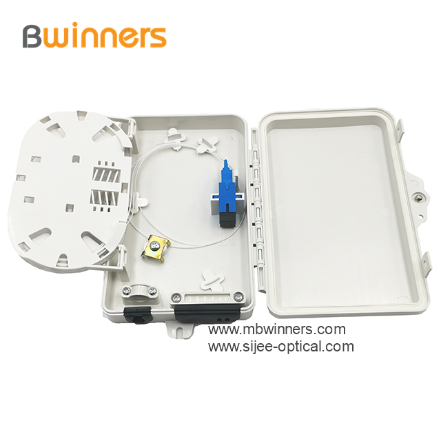
Fiber Optical Distribution Box (Plastic)
Fiber Optic Distribution Box / Fiber Splitter Box is used as a termination point for the feeder cable to connect with drop cable. The fiber splicing, splitting, distribution can be done in this box, and meanwhile it provides solid protection and management for the FTTX network building.
Material: PC+ABS,wet-proof, water-proof, dust-proof, anti-aging, protection grade is IP65.
Small Volume, For Indoor/Outdoor application. Compact structure,convenient installation and maintenance.


Fiber Optical Distribution Box,Plastic Fiber Optical Distribution Box,Fiber Optic Distribution Box,Optical Distribution Boxes
Ningbo Bwinners Optical Tech Co., Ltd , https://www.sijee-optical.com