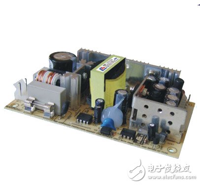
As an energy conversion device operating in a switching state, the voltage and current change rate of the switching power supply is high, and the generated interference intensity is large; the interference source is mainly concentrated during the power switch and the heat sink and the high-level transformer connected thereto, with respect to the number The location of the circuit interference source is clear; the switching frequency is not high (from tens of kilohertz and several megahertz), the main form of interference is conducted interference and near-field interference; and printed circuit board (PCB) traces are usually hand-routed. It has greater randomness, which increases the difficulty of extracting PCB distribution parameters and estimating near-field interference.
Within 1MHZ----based on differential mode interference, increasing X capacitance can solve
1MHZ---5MHZ---differential mode common mode mixing, using input terminal and a series of X capacitors to filter out the differential interference and analyze which kind of interference exceeds the standard and solve it; 5M---the above is mainly based on common touch interference , using a method of suppressing common touch. For the grounding of the case, using a magnetic surround 2 turns on the ground will have a greater attenuation of interference above 10MHZ (diudiu2006); for 25--30MHZ, you can use the larger Y-capacitor and the copper outside the transformer. Change the PCBLAYOUT and the small magnetic ring wound in front of the output line with a minimum of 10 turns, at both ends of the output rectifier and RC filter.
30---50MHZ is generally caused by the high-speed turn-off of the MOS transistor. It can be used to increase the MOS drive resistance. The RCD snubber circuit uses the 1N4007 slow tube, and the VCC supply voltage is solved with the 1N4007 slow tube.
100---200MHZ is generally caused by the reverse recovery current of the output rectifier, which can be used to string magnetic beads on the rectifier
Most of the PFC MOSFET and PFC diodes are between 100MHz and 200MHz. Now the MOSFET and PFC diode string beads have an effect. The horizontal direction can basically solve the problem, but the vertical direction is very helpless.
The radiation from a switching power supply generally only affects frequencies below 100M. It is also possible to add a corresponding absorption loop to the MOS and diode, but the efficiency will be reduced.

Measures to prevent EMI when designing switching power supplies:
1. Minimize the PCB copper area of ​​the noise circuit node; such as the drain and collector of the switch tube, the node of the primary and secondary windings, and so on.
2. Keep the input and output terminals away from noise components, such as transformer wire packages, transformer cores, heat sinks for switch tubes, and so on.
3. Keep noise components (such as unshielded transformer package, unshielded transformer core, and switch tube, etc.) away from the edge of the case, as the edge of the case is likely to be close to the ground wire under normal operation.
4. If the transformer does not use electric field shielding, keep the shield and heat sink away from the transformer.
5. Minimize the area of ​​the current loop: secondary (output) rectifier, primary switching power device, gate (base) drive line, auxiliary rectifier.
6. Do not mix the gate (base) drive feedback loop with the primary or auxiliary rectifier circuit.
7. Adjust the optimized damping resistance so that it does not produce a ringing sound during the dead time of the switch.
8. Prevent EMI filter inductor saturation.
9. Keep the components of the corner node and the secondary circuit away from the shield of the primary circuit or the heat sink of the switch.
10. Keep the node of the primary circuit swing and the component body away from the shield or heat sink.
11. Place the EMI filter of the high frequency input close to the input cable or connector end.
12. Keep the EMI filter of the high frequency output close to the output wire terminal.
13. Keep a distance between the copper foil of the PCB opposite the EMI filter and the component body.
14. Place some resistors on the line of the rectifier of the auxiliary winding.
15. Connect the damping resistor in parallel with the coil of the magnet.
16. Connect the damping resistor in parallel across the output RF filter.
17. Allow 1nF/500V ceramic capacitors or a series of resistors to be connected between the static and auxiliary windings of the primary of the transformer during PCB design.
18. Keep the EMI filter away from the power transformer; especially avoid positioning at the end of the package.
19. Where the PCB area is sufficient, the position of the shield winding and the position of the RC damper can be left on the PCB, and the RC damper can be connected across the shield winding.
20. If space permits, place a small radial lead capacitor (Miller capacitor, 10 picofarads / 1 kV capacitor) between the drain and gate of the switching power FET.
21. Space allows a small RC damper to be placed at the DC output.
22. Do not tie the AC socket to the heat sink of the primary switch.
Linear Actuators,Column Lift Linear Actuator,Motorized Linear Actuator,High Speed Linear Actuator
Kunshan Zeitech Mechanical & Electrical Technology Co., Ltd , https://www.zheteswitches.com