Digital Meters If a 9V battery pack is replaced by a booster with a 1.5V battery, the power switch is usually installed separately. Inconvenience to production and use. The circuit described in this article controls the start or stop by detecting the presence or absence of the digital table operating current. Therefore, as long as the power line is docked with the output of the booster circuit, the digital meter power switch can be used to conveniently control the circuit operation.
The circuit is shown in the drawing. This circuit is a batch oscillation boost circuit. BG1 and L1, L2, C1, etc. constitute an oscillator. BG1 is an oscillating tube and operates in a switching state. L1 and C1 are oscillation feedback elements. L2 is an oscillating energy storage winding. For convenience, the circuit also designed an automatic electronic switch composed of BG3. When the base of BG3 has no load, there is no base current, BG3, BG2, BG1 are all cut off, the whole circuit stops working, and no power is consumed. Therefore, this circuit does not require a separate power switch.
When the two points of A and B are connected to the load, BG3 is turned on, and BG2 is also turned on. The load supplies the base current to BG1, and BG1 is turned on. The energy flows in from the power supply and is stored in L2. At this time, the collector voltage of BG1 is very low, D1 is cut off, and the load is supplied by the residual voltage of C2. When BG1 is turned off, the current in L2 cannot be abruptly changed, and it will produce a higher counter-electromotive force, which is rectified by D1 and output. When the output voltage is higher than the regulation value of D2, the B and e junctions of BG2 tend to be turned off, and the base current of BG1 will decrease, forcing the oscillation to weaken and the output voltage to drop. Thereby the output voltage is automatically controlled near the regulated value of D2.
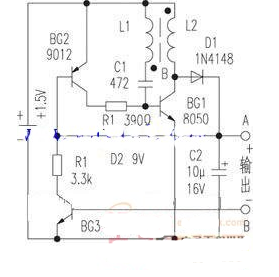
Component selection: BG1 selects NPN type silicon tube with reduced saturation voltage, such as 9013, 8050, etc., requires ICM>300MA, β>200. BG2 can use PNP silicon tubes such as 9012 and 9015, and BG3 uses NPN type tubes such as 9014. The smaller the penetration current is, the better. L1 and L2 are wound on a 高频8MM high-frequency magnetic ring (detached from an old electronic ballast or energy-saving lamp) with a MM0.1MM enameled wire. L1 is 6åŒ and L2 is 36åŒ.
Simple and efficient 1.5v boost circuit diagram (2) MAX1674:Input range 0.9V-5.5V
The output can be fixed at 5V or 3.3V, or between 2V and 5.5V.
DC-DC efficiency can reach 94% at 5V output of 5V

Figure 1 Input 1.5v liter 5v booster with MAX1674
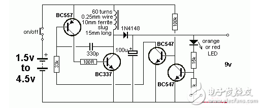
Simple and efficient 1.5v boost circuit diagram (3)Providing an output to a 2.5V to 3.0V circuit will yield approximately 70% efficiency with an output current of 20mA.
The 1.5V liter 9V power supply circuit diagram is shown in the drawing. This circuit is a batch oscillation boost circuit. BG1 and L1, L2, C1, etc. constitute an oscillator. BG1 is an oscillating tube and operates in a switching state. L1 and C1 are oscillation feedback elements. L2 is an oscillating energy storage winding. For convenience, the circuit also designed an automatic electronic switch composed of BG3. When the base of BG3 has no load, there is no base current, BG3, BG2, BG1 are all cut off, the whole circuit stops working, and no power is consumed. Therefore, this circuit does not require a separate power switch.
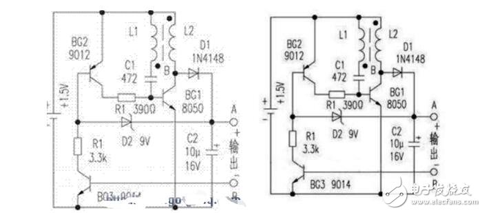
When the two points of A and B are connected to the load, BG3 is turned on, and BG2 is also turned on. The load supplies the base current to BG1, and BG1 is turned on. The energy flows in from the power supply and is stored in L2. At this time, the collector voltage of BG1 is very low, D1 is cut off, and the load is supplied by the residual voltage of C2. When BG1 is turned off, the current in L2 cannot be abruptly changed, and it will produce a higher counter-electromotive force, which is rectified by D1 and output. When the output voltage is higher than the regulation value of D2, the b and e junctions of BG2 tend to be reversed, and the base current of BG1 will decrease, forcing the oscillation to weaken, and the output voltage will also drop to automatically output the voltage. Control is near the regulation value of D2.
Component selection and production debugging:BG1 selects NPN type silicon tubes with reduced saturation voltage, such as 9013, 8050, etc., and requires ICM"300mA, β"200. BG2 can use PNP silicon tubes such as 9012 and 9015, and BG3 uses NPN type tubes such as 9014. The smaller the penetration current is, the better. L1 and L2 are wound on a 高频8MM high-frequency magnetic ring (detached from an old electronic ballast or energy-saving lamp) with a MM0.1MM enameled wire. L1 is 6åŒL2 is 36åŒ.
I use this circuit to supply power to the DT890A digital multimeter. The measured working current is: buzzer and capacitor 20uF, 2uF block is below 45mA, other gears are below 25mA. When the battery voltage drops to 0.9V, in addition to the buzzer block that consumes a large current, the capacitors 20uF and 2uF block have a power shortage display, and the remaining gears have no power shortage display. The circuit is simple to manufacture, stable in performance, economical and practical. No need to debug, as long as the wiring is correct, it can work normally.
Digital Multimeters If a 1.5V battery is used to replace a 9V stacked battery with a boost, it is usually necessary to install a separate power switch. Inconvenience to production and use. The circuit described in this article controls the start or stop by detecting the presence or absence of the digital multimeter's operating current. Therefore, as long as the power line is connected to the output of the booster circuit, the digital multimeter power switch can be used.
Simple and efficient 1.5v boost circuit diagram (5)The booster circuit described in this paper has a small operating current. It is only about 6 mA at no load. When the working current is lmA~3 mA digital multimeter, the battery current consumed is between 15 mA and 30 mA. In Fig. 3, 8050 and 8550 constitute a self-excited oscillator, and the back electromotive force of the inductor connected to the collector of Q2 is rectified to form a high voltage. The voltage level is determined by the Zener diode D1. When the output voltage exceeds the breakdown voltage of the Zener diode, the Zener diode is turned on, the base voltage of Q1 rises, the Q2 current is reduced, and the output voltage is stabilized at 9V. Replace the Zener tube to change the output voltage. To meet the needs of other occasions, the maximum output voltage can reach 50V under no-load conditions. The inductor L is wound with a magnetic core of 7mm×7mm mid-week, wrapped with a Φ0.1mm enameled wire on the I-shaped magnetic core, and then wrapped in a layer of tape and then inserted into the magnetic cap, sealed on the circuit board with glue, two The terminal can be connected to the circuit.
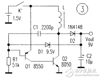
With load capacity is very good, using 9013 can meet most digital meters, if it is a relatively power-consuming digital meter, you can replace 9013 with a special flash tube such as D965, and the winding of the transformer connected to the collector should use a thicker enameled wire. The feedback and boost windings are unchanged, and it can be used with 0.08mm.
The following figure is with a high voltage protection diode to prevent Q1 ce short circuit or D1 open circuit to make the circuit run out of control to generate high voltage, damage the digital meter.
The enameled wire was used in the original mid-week. Generally it is 0.07 ~ 0.08mm, and the TTF-2 has more than 140 turns in the middle of the week, which is enough. The winding direction can be forward or reverse, but all windings must be in the same direction.
The double wire is wound 30 times to reduce the skin effect and resistance. It can also be used with 0.16mm enameled wire. The effect is the same.
Rewinding 50 ---- 70 T is to output enough voltage after the battery voltage drops. In actual use, it will be found that when the multimeter shows low voltage, the battery has been completely discharged, and the short-circuit output current is less than 30mA.
9013 can be replaced by 3DX201, 3DX203, hFE is greater than 150, 9014 is used for 3DG201, 3DG202, 3DG6, etc. 9015 is used with any small power tube of 3CG type, generally hFE is greater than 80. Note that the penetration current must be small, otherwise the circuit cannot be automatically turned off.
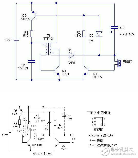
The advantage of using the radio mid-week is that the electromagnetic shielding effect is better, and the external interference is small. The manufactured transformer has a high Q value and high work efficiency.
In fact, it can also be made of other materials, such as a small magnetic ring in an energy-saving lamp, a 300/75 impedance matching double-hole magnetic core in a TV antenna (three on the antenna amplifier), as long as it can be wound up, a thick enameled wire Better.
Generally, the primary level of the oscillating tube can be used with a slightly thin enameled wire, around 10 to 20 turns, the secondary line is slightly thicker, and around 20 to 30 turns, the boosting winding can be removed, because the rechargeable battery is now used, no need to extract The last bit of energy in the battery.
Simple and efficient 1.5v boost circuit diagram (7) 1.5V battery powered 15V output DCDC boost circuit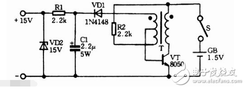
The resistance DC component magnetic core has strong resistance DC component ability, wide current range, few additional circuits and devices,strong reliability and insensitive to interference. Our company produces two kinds of resistance DC component magnetic cores: single core and composite core. The composite core adopts double core design, which has lower cost than cobalt based alloy. It has high permeability,low coercivity and loss,excellent performance on DC immune and temperature stability that can be widely used to the electronic watt-hour meter,resistance DC component transformer and electrical power system measurement.
Anyang Kayo Amorphous Technology Co.,Ltd. , https://www.kayoamotech.com