In the previous section, we theoretically analyzed the generation of EMI, and considered many practical methods and methods for suppressing EMI from the perspective of system design. In this section, we will analyze how to perform EMI control for high-speed PCB design.
1 transmission line RLC parameters and EMI
For PCB boards, each trace on the PCB can be described by three basic distribution parameters, namely resistors, capacitors and inductors. In the control of EMI and impedance, the inductance and capacitance play a great role.
A capacitor is a component of electrical energy stored in a circuit system. Capacitance may be formed between any two adjacent transmission lines between the two layers of PCB conductive layers and between the voltage layers and the surrounding ground plane. Among all these capacitors, the capacitance between the transmission line and its return current is the largest and the largest, because any transmission line will form a recirculation around it by some kind of conductive material. According to the formula of the capacitance: C = εs / (4kπd), the size of the capacitance formed between them is inversely proportional to the distance from the transmission line to the reference plane, and is proportional to the diameter (cross-sectional area) of the transmission line. We all know that if the value of the capacitor is larger, then the electric field energy stored between them will be more. In other words, the ratio of energy leaking to the outside system will be less, then the EMI generated by this system will get a certain amount. Inhibition.
An inductor is an element in a circuit system that stores the energy of the surrounding magnetic field. The magnetic field is the induced field created by the current flowing through the conductor. The value of the inductor indicates its ability to store the magnetic field around the conductor. If the magnetic field is weakened, the inductive reactance will become smaller. When the inductive reactance becomes larger, the magnetic field will increase, and the external magnetic energy radiation will also become larger, that is, the EMI value. The bigger. Therefore, if the inductance of the system is smaller, EMI can be suppressed. In the case of low frequency, if the conductor becomes shorter, the thickness becomes larger, and when the width is wider, the inductance of the conductor becomes smaller, and in the case of high frequency, the magnitude of the magnetic field is a function of the closed-loop area of ​​the wire and its reflow, If the wire is close to its loop, since the reflow and its own current are equal in magnitude (in the optimal reflow state), the magnetic fields generated by the two cancel each other out, reducing the inductance of the conductor, so the current on the conductor and its The optimal return path can reduce EMI to a certain extent.
In an actual circuit, the capacitance and inductance of the wire are integrated. If we only analyze the capacitance or only consider the inductance, it is one-sided, so we introduce the impedance. The impedance is the ratio of the input voltage to the input current on the transmission line (Z0=V/I). The impedance between the wire and the loop is a function of the inductance and capacitance between the wire and its loop, and the impedance ZO is equal to (L/C) 1/2. .
From the previous analysis and the formula of the impedance ZO, from the viewpoint of suppressing EMI, we hope that the impedance is as small as possible. When the impedance is small, that is, the capacitance is large and the inductance is small, we can keep the EMI control to a minimum as long as the circuit is properly wired and the current is kept at the optimum return path. When the capacitance becomes smaller and the inductance becomes larger, the ability of the system to shield the electromagnetic field energy is reduced, the energy of the leakage electromagnetic field is increased, and the EMI is increased.
2 laminate design suppresses EMI
As can be seen from the previous analysis, the low-impedance reference plane plays a crucial role in suppressing EMI. Therefore, we should pay special attention to the arrangement of the reference plane layer when designing the laminate. For signal traces on the PCB, good stratification should be such that all signal layers are next to the power or ground plane; from the power supply, good stratification should be adjacent to the ground plane. And the distance between the power supply and the ground plane is as small as possible to ensure low impedance on the power supply and the ground. As the signal frequency continues to increase, generally only a multi-layer PCB board with more than 6 layers can achieve good EMI suppression. Below, we take 6-layer board as an example to compare the performance of different PCB laminate design schemes.

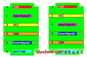
Figure 1. Two typical laminate designs for a six-layer PCB
There are usually two options for the stack design of a six-layer PCB (as shown in Figure 1). For the first option, we can place the power supply and ground on the 3rd and 4th layers respectively. Although the power supply copper has low impedance, the electromagnetic shielding performance is poor because the first layer and the sixth layer are signal layers. A large part of the magnetic field on the wire is radiated to the outside. In other words, one of the signal current and the return signal is in the shielding range, and the other half is outside the shielding range, and one is within the shielding range. In fact, the differential mode EMI has been added. However, if the number of signal lines on the two outer layers is the smallest and the trace length is short (less than 1/20 of the highest harmonic wavelength of the signal), this design can solve the differential mode EMI problem. The suppression of differential mode EMI is particularly good when copper is filled with no components and no trace areas on the outer layer and the copper area is grounded (interval every 1/20 wavelength). Moreover, we can also lay a circle of copper at the edge of each layer of the signal layer under the condition of the condition, and control it within the interval of 1/20 wavelength, which can also prevent EMI leakage. The copper area should be connected to the internal ground plane. The second solution is to place the power supply and ground on the 2nd and 5th layers respectively. Although most of the differential mode EMI is suppressed, the high-voltage copper-clad impedance is not good for reducing common-mode EMI radiation. In addition, signal impedance
From a control point of view, this approach is also very beneficial, so the program has become the most widely used six-layer board design.
If we have the ability to distribute all the signal traces completely within two layers, then we can use other more optimized laminate designs: laying layers 1 and 6 (two skins), 3rd and The 4th floor is set to power and ground. The signal line runs on the 2nd and 5th layers, and both sides have a reference plane shield, so the EMI suppression capability is excellent. The disadvantage of this design is that the wiring layer has only two layers, and the wiring space is slightly tight. In practice, it should be handled flexibly. For example, it can be properly routed in the copper-plated area, but it should be noted that the return path of the upper layer signal cannot be blocked.
There is also a stacking scheme: signal, ground, signal, power, ground, and signal, which also achieves a good environment for signal integrity design: the signal layer is adjacent to the reference layer, and the power plane and ground plane are paired. The downside is that the stack of copper layers is unbalanced, which can cause troubles in manufacturing. The solution to the problem is to fill all the blank areas of the third layer with copper. If the copper layer density of the third layer is close to the power layer or the ground layer after copper filling, the board can be regarded as a structurally balanced circuit board. . Note that the copper-filled area must be connected to a power source or ground (preferably grounded), and the distance between the connected vias is still less than 1/20 wavelength.
3 Capacitance and ground vias for reflow
The suppression of EMI in high-speed PCB design is very flexible. Designers can never solve all EMI problems perfectly. Only from a small place, from the grasp of various details to achieve the overall suppression effect, sometimes, often look A seemingly insignificant capacitor or via can play a decisive role. It may be mentioned that the suppression of EMI by capacitors is familiar to everyone, that is, the storage characteristics of the capacitors are used to stabilize the voltage and eliminate the higher harmonics, thereby reducing the EMI effect. In this section, we will focus on the role of capacitors and ground vias in ensuring low-impedance loops in signals, which is one of the important aspects of effective EMI suppression in multilayer PCB designs.
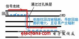
In multi-layer PCB design, due to wiring density and topology requirements, signal traces often need to be switched between layers. If the ground plane to which it is referenced also changes, the return path of the signal will change, resulting in a certain The EMI problem is shown in Figure 2:

Figure 2 EMI problem caused by signal layer change
The easiest and most effective way to solve this problem is to add capacitors or vias reasonably. If two different reference planes are ground or both, then we can provide a loop for the return of the signal by adding a ground via or a power supply via (Figure 3 A); if the two reference planes are power and ground Switching between them allows the use of bypass capacitors to provide a low impedance loop (Figure 3 B).

Figure 3 Via or capacitor provides a return path
In the above figure, we can see that some ground vias (power supply holes) and capacitors are placed near the signal trace layer to provide a complete low-impedance loop for the signal, ensuring coupling between the signal and the reflow, thereby suppressing EMI. It should be noted that when the reference plane is switched by the capacitor through the capacitor, due to the parasitic inductance of itself and the via, there will still be some electromagnetic radiation and signal attenuation. Therefore, the designer must have a correct guiding idea: try to change as little as possible. Layer routing, try to keep the signal close to the same (or the same attribute) reference plane after changing layers.
Trench Cover,Trench Drain,Drain Cover,Steel Trench Covers
Hunan Furui Mechanical and Electrical Equipment Manufacturing Co., Ltd. , https://www.thresher.nl