one. research background and meaning
With the introduction of the smart grid concept, energy metering and marketing solutions based on home smart interactive terminals have gradually formed, which means that home control will move towards intelligence. Smart home is a new type of home that has been produced and rapidly emerged in recent years. The intelligentization of home provides residents with a safer, more comfortable, convenient, fast and open intelligent and informational living space. Convenient for the user. Therefore, the establishment of a home control system with family interactive terminals as the core is of great significance to the transformation and implementation of smart grids.
However, the current home intelligent system has a big limitation, that is, it only achieves partial intelligence. In the true sense of home intelligence, it should have a centralized terminal control system, through which the intelligent control and monitoring of all the devices in the home will be the future development direction of the smart home system.
This design uses MIPS' 32-bit processor as the core to build an intelligent display terminal, and uses a smart socket with wireless communication as the controlled node to build a simple smart home control system. The system can be controlled by remote (mobile phone text message) and local (smart display terminal). The following is an analysis of the composition and implementation of the system, as well as the key issues involved in each module.
two. System composition and working principle
1 System structure and principle
The system consists of a mobile phone, an intelligent display terminal, and a smart socket. The mobile phone communicates with the intelligent display terminal through the GSM module, and the Zigbee is used for communication between the intelligent display terminal and the smart socket.
As a basic control unit, the smart socket can collect the electricity usage information of each room in real time and transmit the information to the intelligent display terminal in real time. When a power abnormality is found, the smart socket automatically powers off and sends the execution result to the smart display terminal. The intelligent display terminal also sends this result to the user's mobile phone.
The mobile phone realizes remote control and information reception of the user. When the user goes out, the commands sent by the mobile phone (such as pre-boot, pre-shutdown, time-limited power supply, etc.) will be received by the smart terminal and delivered to the smart socket. In addition, all execution actions of the smart socket will be sent to the mobile phone through the smart display terminal.
The intelligent display terminal can receive the commands sent by the mobile phone as well as the data sent by the smart socket. After the smart display terminal accepts the data uploaded by the smart socket, the data will be stored. When the user starts the query function, the intelligent display terminal will call the data and perform analysis and calculation to display various types of power consumption information.
2 Function introduction
1 Real-time power monitoring
2 Pre-start and pre-shutdown of the appliance
3 limited time power supply
4 limited power supply
5 temperature monitoring
6 fault alarm
7 SMS remote control
8 local touch screen manipulation
9 various types of query functions. Including monthly electricity, daily electricity, electricity during the period, accumulated electricity at any time, and the electricity consumption of any single appliance.
10 user-friendly touch screen operation and voice output
three. Project technical plan
1 system composition
The system equipment is mainly composed of three parts: mobile phone, intelligent display terminal, and smart socket. As shown in Figure 1.1.
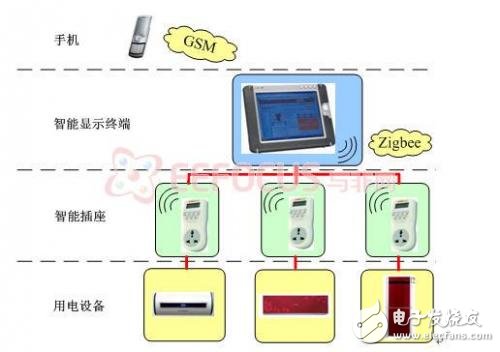
Figure 1.1 System schematic
1.1 System Structure
The system equipment is mainly composed of three parts: mobile phone, intelligent display terminal, and smart socket.
According to whether the head of the household is at home, two ways are designed for control.
1 SMS message. This method is mainly designed for the situation where the head of the household is on a business trip, which is convenient for remote control. The mobile phone can send a command to the smart display terminal, and after receiving the command, the smart display terminal decodes the command and sends a command to each smart socket. After receiving the control command, the smart socket performs the corresponding operation, and feeds back the execution result to the intelligent display terminal, and the smart display terminal sends the received information to the mobile phone.
2 local touch screen. This approach is designed for the situation of the head of the household. The owner can directly complete the corresponding operation on the touch screen and control according to the interface prompts.
The intelligent display terminal and the mobile phone communicate through the GSM module, and the intelligent display terminal and the smart socket communicate with each other through Zigbee.
The system block diagram is shown in Figure 1.2:
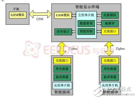
Figure 1.2 Overall system block diagram
1.2 Functional Description
1 Through the system, real-time monitoring of home appliances, timed start, limited power supply and other important functions can be realized, and the electrical equipment in each room can be easily managed.
2 Through the smart socket and wireless communication on the intelligent display terminal, the user can view the detailed power consumption information of each power device in the home. Users can query the monthly electricity consumption of each device for each month, every day, or even for a certain period of time.
3 local remote operation. Even if you are on a business trip, you can know the power usage in your home. The functions implemented by each part are shown in Figure 1.3:
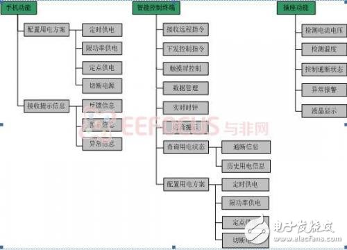
Figure 1.3 System function block diagram
2 key module analysis
This design is intended to use the 32-bit control chip of the Digilent CerebotTM 32MX4 development board. The key feature of the Cerebot 32MX4 is a new Microchip® PIC32TM microcontroller. The PIC32 provides a 32-bit MIPS processor core operating at 80MHz, 512KB of programmable FLASH, 32KB of RAM memory, and numerous peripherals including USB controllers, timer/counters, serial controllers, A/D converters, and more. More equipment.
The board has a large number of I/O interfaces to meet the needs of this system, and the USB power supply and built-in programming compatible with Microchip's MPLAB development software make debugging circuitry very convenient.
The RTCC and AD circuits in this system use the built-in modules of the MCU, and do not need to be designed separately. The software and hardware design of other modules are analyzed below.
2.1 GSM module analysis
2.1.1 Hardware Design
The GSM short message service SMS uses signaling channel transmission to provide a guaranteed two-way service, which is unique to the GSM communication network. It does not dial to establish a connection, sends the information to be sent plus the destination address to the short message service center, and then stores it and then sends it to the final sink. Therefore, the information will not be lost even when the destination GSM terminal is not turned on. After the sender sends a short message, it gets a message that the success or failure is delivered, and the reason for the unreachable. The amount of information per short message is limited to 140 bytes.
At present, the technology of GSM chip and GSM transceiver module has been relatively mature, and ready-made modules are available in the market. These chips and modules generally have all the functions of GSM wireless communication, provide standard RS-232 interface, support the command of AT command set defined by GSM07.05, it is easy to realize system integration, secondary development is also more convenient, this The design chose a cost-effective Siemens MC39i wireless transceiver module.
The MC39i is Siemens' next-generation dual-band GSM/GPRS wireless module, which is an environmentally-friendly upgrade of the widely used MC39i module. Its compact design provides users with a simple, in-line wireless connection. The MC39i is rich in AT commands, powerful, flexible and convenient. It is a kind of data terminal equipment combining traditional modem and GSM wireless mobile communication system. The module integrates the RF circuit and the baseband to provide users with a standard AT command interface to provide fast, reliable and secure transmission of data, voice, short messages, and faxes, facilitating user application development and design.
Main performance:
Support EGSM900/GSM1800 dual frequency;
Suitable for GSM2/2+;
Output power: power level 4 (2W), EGSM900; power level 1 (IW), GSM1800;
Data transmission GPRS mode;
The maximum downlink transmission rate is 85.6 kbps;
The maximum uplink transmission rate is 42.8 kbps;
Standard RS232 bidirectional interface;
AT command control;
The power supply voltage is a single voltage of 3.3 to 4.8V;
Current consumption: 3.0 mA (sleep), 10.0 mA (idle)
The internal block diagram of the MC39i module is shown in Figure 2.1. It is mainly composed of four parts: GSM baseband processor, GSM radio frequency part, power supply and memory. The GSM baseband processor is the core of the whole module. It controls the transmission, conversion and amplification of various signals in the module by a C166CPU and a DSP processor core. The GSM radio part is a single-chip transceiver consisting of a heterodyne receiver, an up-conversion modulation loop transmitter, an RF phase-locked loop and a fully integrated IF synthesizer. Processing such as reception and transmission of signals.
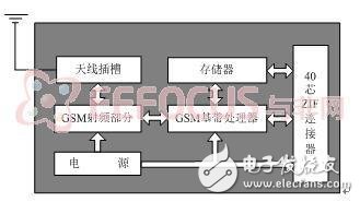
Figure 2.1 Mc39i block diagram
The main hardware design of this module includes the following two parts.
1 User identification card (SIM card).
The Mc39i's baseband processor integrates a SIM interface that is compatible with the ISO 7816-3 IC Card standard. In order to fit the external SIM interface, the interface is connected to pins 24 to 29 of the Mc39i via a ZIF connector. The Mc39i has six pins reserved for the SIM card interface on the ZIF connector. The added CCIN pin is used to detect if a SIM card is inserted in the SIM card holder. When the SIM card is inserted, this pin is set high and the system can enter normal operation.
2 SYNC signal and circuit design.
The SYNC signal is used in this circuit design to control a status light to detect what state the MC39i module is currently in. Due to the insufficient drive capability of the SYNC pin output of the MC39i module, the design uses a triode to amplify the input current to improve drive capability.
Some hardware design diagrams are as follows:
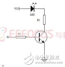
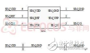
Figure 2.2 Schematic diagram of the SYNC signal
Figure 2.3 SIM card interface
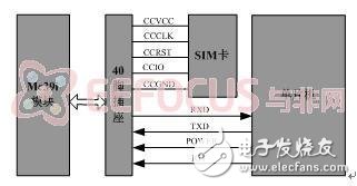
Figure 2.4 GSM part hardware block diagram
2.1.2 Software Design
The PDU Mode PDU mode of the SMS short message using the AT command is a method of transmitting or receiving SMS information of the mobile phone. The PDU string is a string of ASCII codes on the surface, and the numbers are from '0' to '9' and 'A' to 'F'. And letters. They are 8-bit hexadecimal numbers, or BCD code decimal numbers. The PDU string contains not only the message itself, but also many other information, such as SMS service center number, destination number, reply number, encoding method and service time. The short message body is transmitted after being hex encoded.
A PDU is equivalent to a data packet, which consists of information that constitutes a message (SMS). As a single element of data, it must contain the source/destination address, protection (valid) time, data format, protocol type, and body. The body length can be up to 140 bytes, all of which are expressed in hexadecimal. The PDU structure differs depending on whether the short message is initiated by the mobile terminal or for the purpose of the mobile terminal.
1 When the mobile terminal initiates, the format of the PDU is:
SMSC PDU Type Pulse DA PID DCS VP UDL UD (0~1400cted)
2 For the purpose of the mobile terminal, the format of the PDU is:
SMSC PDU Type OA PID DCS SCTS UDL LID (0~400cted)
The SMSC is the short message service center address, the DA/OA is the source/destination address, the PID is the protocol identification, the DCS is the data encoding, the UDL is the user data length, the UD is the user data, the VP is the valid time, and the LID indicates the sending information. , SCTS indicates when the short message arrives at the business center.
The short message sent in the system contains Chinese characters and numbers, so the user information encoding mode TP-DCS of the PDU string is 08, indicating the UCS2 encoding mode, and the UCS2 encoding is to match each character (1-2 bytes) according to ISO. /IECl0646 provisions, converted to 16-bit Unicode wide characters. However, in the GSM standard, Chinese encoding uses UTF-8 encoding, which is not the commonly used GB-2312 encoding in China. Therefore, it is necessary to convert Chinese encoding to display Chinese fonts in conjunction with GB-2313 Chinese character library. Since there is no one-to-one linear relationship between UTF-8 and GB-2312 encoding, it can only be converted by looking up the table.
Before the message is sent, the ASCII characters and Chinese characters in the message are uniformly encoded into UCS2 code and sent in the form of PDU data packets. The received data is stored in the Mc39i module or SIM card in the encoded form of 7b. When the data is read, the data conforming to the GSM specification is directly obtained from the Mc39i module, and the useful data of the 7b code is extracted. However, these 7b encoded data exist in the form of ASCII characters, which are converted into 8-bit hexadecimal 7b codes, and then decoded into usable ASCII code data, thus obtaining the original data sent by the GSM network, such as Figure 2.5 shows.

Figure 2.5 SMS data transmission process
After the MC39i is powered on, first select the port, then check if the SIM is inserted. After successfully detecting the SIM card, the serial port can be sent and the status light is illuminated. Then set the short message center and perform the connection test. After the connection is successful, send the startup success message to the main controller. If the above steps are not executed successfully, then the error processing is turned. The working flow chart of the Mc39i module is shown in Figure 2.6.
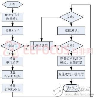
Figure 2.6 Mc39i work flow chart
2.2 Zigbee communication module analysis
Zigbee is a low-speed short-range wireless communication technology. It is a scalable, easy-to-build low-cost wireless network with low power consumption and two-way transmission. It is suitable for automatic control and remote control and can be embedded in various devices. It has been widely used in the field of home automation.
Zigbee technology has the following characteristics:
n Power saving. Due to the short duty cycle, low power consumption of the transceiver, and the sleep mode.
n The time delay is short. The device search latency is typically 30 ms, the sleep activation delay is typically 15 ms, and the active device channel access delay is 15 ms.
The n-node communication settings are easy to configure.
n Close range. The transmission range is generally between 10 and 100 m.
n Network capacity is large. Zigbee can be networked in star, mesh, or string structure, and can be connected to form a larger network structure through any node.
n Security. Zigbee provides data integrity checking and authentication. The encryption algorithm uses AES128, and each application can flexibly determine its security attributes.
n Global versatility and openness. The Zigbee standard protocol makes communication between Zigbee devices a breeze.
In this system, smart sockets and intelligent terminals need to communicate wirelessly, transmit commands or data in both directions, and then control home appliances. Zigbee is a low-power, low-cost wireless method that conforms to the energy-saving concept of home systems. Zigbee's data transfer is not large, and our command data is also a short packet, enough to meet the demand. In addition, Zigbee's secure, open protocol approach makes it easy to expand devices on this basis, which also lays the foundation for the diversified development of smart homes.
2.2.1 Hardware design
The system determines the range of the detection area by a plurality of terminal nodes (smart sockets), and the power consumption data monitored by each terminal node is transmitted to the intelligent display terminal for processing through the self-organized multi-hop network. The commands sent from the SMS platform or the touch screen are decoded and decoded by the intelligent display terminal, and thus broadcasted to each smart socket.
1, chip selection
This scheme adopts CC2430 as the core structure data acquisition node. It only needs to connect a small number of passive components such as crystal oscillator, capacitor and resistor to the CC2430 chip, which can not only meet the requirements of data acquisition, wireless communication and other functions of the whole system, but also has low power consumption. The circuit is simple, the node is small in size and low in cost.
2, networking structure
The Zigbee network supports three network topologies: star, tree and mesh.
The star network consists of a ZigBee coordinator and multiple terminal devices. There is only communication between the ZigBee coordinator and the terminal device. The terminal devices cannot communicate directly. They need to be forwarded by the ZigBee coordinator. The tree network consists of a ZigBee. The coordinator is connected with multiple star-shaped structures, and the flexibility is higher than that of the star topology. The mesh structure is the most complete, and the nodes in any network can be interconnected, and the traffic is also the largest, but the storage space overhead is too large.
Considering that the number of devices in this system is small and the network complexity is not high, it is proposed to adopt a more economical star structure.
In this system, the intelligent display terminal is a coordinator (ie, a master node), and the smart socket is a device terminal (ie, a child node). The hardware block diagram is shown in Figure 2.7:
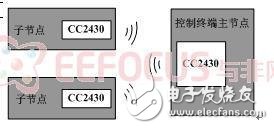
Figure 2.7 node hardware design block diagram
72V20Ah Lithium Ion Battery,Electric Scooter Lifepo4 Battery Pack,Lithium Battery For Electric Motorcycle,Lithium Battery For Electric Bike
Jiangsu Zhitai New Energy Technology Co.,Ltd , https://www.jszhitaienergy.com