The three-dimensional magnetotelluric exploration technology is based on the face unit, the multi-component acquisition station as the center, and the characteristics of how far reference, cross-reference and densely arranged points are used to obtain high-quality acquisition data. In the field construction, in order to keep the data collection synchronized between the sites, the GPS second pulse signal or the timing signal of the constant temperature crystal oscillator is generally used to synchronize the collection sites. The former will often jump due to various interferences in the harsh construction environment, and the synchronization effect is not ideal. The latter has frequency drift for a long time, and it is also unable to maintain long-term synchronous acquisition.
In order to solve the above problems, this article uses GPS timing signal to calibrate the voltage-controlled crystal oscillator of each site, and then uses the crystal oscillator frequency division to obtain the timing signal to synchronize each acquisition site. This not only overcomes the shortcomings of GPS timing signals that are susceptible to external interference, but also solves the problem of crystal oscillator frequency drifting with time, and can obtain a more ideal synchronization signal. In order to synchronize the local crystal oscillator with the GPS system for a long time, it is necessary to continuously measure the time interval between the GPS timing signal and the frequency division signal of the local crystal oscillator, and then calibrate and synchronize the local crystal oscillator according to the measured data. Therefore, the accuracy of time interval measurement is the key to ensuring the performance of the frequency calibration system. Based on the characteristics of high integration, high speed and high reliability of FPGA, this paper introduces the design method of crystal oscillator frequency calibration system in FPGA. The system is characterized by the use of FPGA internal carry logic to construct a delay line to achieve time interval measurement, which greatly improves the measurement resolution. At the same time, it uses the FPGA embedded soft core processor PicoBlaze to monitor the system status and filter the measurement data. Give full play to the integrated advantages of FPGA.
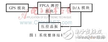
1 System design 1.1 System implementation schemeThe principle of the system is shown in Figure 1. It is mainly composed of 4 parts: GPS receiving module, FPGA measurement and control module, D/A conversion module and voltage-controlled constant temperature crystal oscillator. The GPS receiving module is used to output standard 1-pps pulse signals, and the FPGA measurement and control module is used to measure the time interval between the local crystal oscillator frequency division signal and the 1-pps signal, and process the measured value in PicoBlaze to obtain the crystal oscillator output frequency relative to The frequency deviation of the GPS system is finally used as the input of the D/A conversion module to obtain the control voltage for correcting the frequency of the local crystal oscillator.
The principle of time interval measurement in FPGA is shown in Figure 2. The 1-pps second pulse signal is compared with the 100 kHz signal obtained by the local crystal oscillator frequency division. The time difference obtained is the time interval to be measured. Since only the time interval between the rising edges of the two is sampled, the 100 kHz frequency-divided signal is used to replace the 1 Hz second signal for comparison with 1-pps, which can reduce the measurement value each time and facilitate data processing. It should be noted that the time difference range of the crystal oscillator relative to 1-pps must be within one cycle of the 100 kHz signal, that is, the frequency of the signal determines the size of the measurement range, and the frequency of the signal can be determined according to the actual measurement needs.
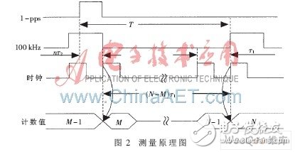
In Figure 2, T is the time interval to be measured, τ1 is the counting clock period, M is the count value of the counter when the 1-pps signal arrives, N is the count value of the counter when the 100 Hz signal arrives, and nτ2 is due to 1-pps The measurement error caused by the inconsistency between the rising edge of the pulse and the rising edge of the counting clock is measured by the interpolation delay line. Since the 100 kHz signal is obtained by dividing the frequency of the crystal oscillator, it is synchronized with the counting clock, so there is no measurement error. Therefore, the time interval to be measured can be expressed as:

In order to calibrate the local crystal oscillator in a short time and synchronize it with the GPS system, the measurement resolution of the time interval must be improved, and the time interpolation technique is used in the design. The basic principle is to use multiple delay units to construct a delay line, and the propagation information of the signal under test in the delay line can be used for time interval measurement. The realization of the delay line mainly depends on the uniformity of the delay of the interpolation delay unit. The unit delay of the interpolation delay unit determines the resolution of the time interval measurement system. To implement time interpolation in FPGA, the key is to construct a delay line based on its structure using internal existing resources
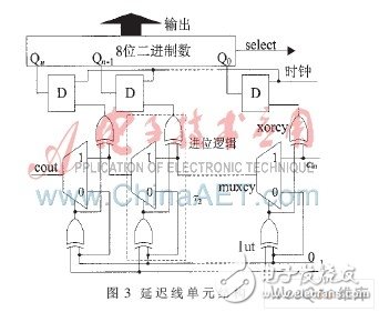
In the unit structure of FPGA of XILINX Company, in order to realize the fast mathematical operation, set up a lot of dedicated carry logic resources. The delay of these carry logics is very small, and they can be connected to each other to form a carry line, and this special carry line can be used as a delay line to implement time interpolation. As shown in Figure 3, the dedicated carry logic in the Spartan-3 series FPGA is used in the design to connect one by one to form a delay line. A carry logic consists of a look-up table (LUT), a dedicated gate (MUXCY) and a dedicated exclusive OR gate ( XORCY) consists of three parts. The overall structure is similar to a multi-bit binary adder. The bits of the two inputs are set to 1 and 0 respectively. When the carry signal does not come, the bits of the adder are all 1. When the carry signal arrives, it will be transmitted level by level along the carry line. The change in the output value of each adder represents the delay information of the signal. When the leading edge of the clock arrives, this information can be latched into the flip-flop . Figure 4 shows the number of delay units that the delay line unit output passes through in the simulation of one clock cycle. The result after the straight-line fitting is:
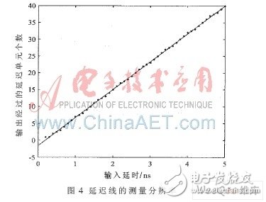

Therefore, the measurement resolution of the delay line unit is about 1/8.257 4=0.121 ns.
1.4 The design of the counter moduleFigure 5 briefly describes the basic structure of the counter module. In the design of the counter module, the digital clock manager of the Spartan-3 series is used. The main purpose is to multiply the crystal oscillator clock signal as the working clock of the counter to ensure that the clock period is less than the total delay of the delay line. According to the measurement resolution and length parameters of the delay line unit determined by the timing simulation, the crystal oscillator frequency is multiplied to 200 MHz.
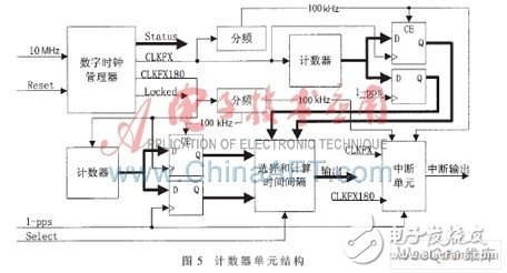
The counter output near the leading edge of the clock is in a metastable state. If the 1-pps signal arrives at this moment, the wrong count value will be latched. In order to solve this problem, the digital clock manager is used in the module to output two clocks with a phase difference of 180°, and respectively drive two counters to work at the same time, so that the output of one of them can be guaranteed to be the correct value at any time, and then correct Both make a judgment choice. The selection signal is provided by the delay line unit, and the time difference between the 1-pps signal and the leading edge of the clock is determined by counting the number of the 1-pps signal passing through the delay unit, and then the select signal is output.
Two counters perform cycle counting, and each counter is connected to two sets of registers, one of which uses the GPS second pulse signal as the working clock; the other set of clock signals is connected to the clock of the corresponding counter, and its enable terminal is connected to 100 The kHz crossover signal is connected. When the GPS second pulse and 100 kHz signal arrive, the count value will be sent to the corresponding register group. This can make full use of the FPGA's global clock resources, so that the corresponding register groups all use the same clock, and the synchronization of register triggers is guaranteed. In addition, the use of cycle counting also solves the problem of counter output errors caused by the traditional start-stop counter because the start and stop signals do not meet the set-up and hold time. When the leading edge of the 1-pps signal and the 100 kHz signal are reached, the interrupt unit will output an interrupt signal to notify the PicoBlaze soft core to read the measurement result.
1.5 PicoBlaze soft core designPicoBlaze is an 8-bit microcontroller soft core designed by XILINX. It can be embedded in the CPLD and FPGA of Cool Runner II, Virtex-E, Virtex-II (Pro) and Spartan 3 (E), and the design is flexible and convenient. The port bus of PicoBlaze provides 8-bit address (PORT_ID) and read and write strobe signals, which can realize up to 256 input and output ports. The interface design is shown in Figure 6. PicoBlaze is used to receive the output results of the delay line module and the counter module, and read the data and status information of the asynchronous serial controller (UART) at the same time. Among them, the asynchronous serial controller directly calls the IP core of XILINX to carry out serial communication with the external GPS module.
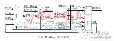
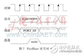
In addition, in order to realize the storage of measurement data to facilitate data processing, PicoBlaze connects a FIFO data buffer to temporarily store unprocessed measurement data. As shown in Figure 7, each read and write operation of PicoBlaze requires two clock cycles. During this period, the address bus is always in a valid state, and the read and write enable signal is only valid in the second clock cycle, so the address bus can be properly connected The logic circuit performs address decoding.
In the design, four gates are used to connect the output of the counter module, the delay line module and the FIFO buffer respectively. Because the counter module adopts a 16-bit counter cycle counting, in order to match the PicoBlaze input, the count value must be divided into two parts. Strobe. The output and status information of the asynchronous serial controller are respectively connected to the three-way gate, and the remaining one is connected to the output of the four-way gate. Because the clock frequency and measurement part used by UART and PicoBlaze are different, in order to improve the reliability of data transmission, a pipeline register is added between the strobes.
When the system is running, PicoBlaze will query the UART status, and when it detects GPS serial code data, it will start to read its serial code information. The GPS serial code information is used to analyze the current GPS status. If it is detected that the GPS module has locked the satellites, the system will start measurement and calibration.
2 Measurement data processingAccording to the measured time interval data, according to the formula:

The frequency deviation of the crystal signal relative to the GPS can be calculated, where T1 and T2 are respectively the time interval measurement values ​​output before and after the sampling time τ of the measurement part. According to the size of the frequency deviation, combined with the voltage control sensitivity of the crystal oscillator, the output frequency of the crystal oscillator can be controlled and corrected. However, GPS signals are susceptible to external influences during transmission. The 1-pps signal output by the GPS module is a fluctuating signal, and its short-term stability is poor. The black curve in Figure 8 is the time interval curve of the local crystal oscillator relative to the GPS system measured by this system. The frequency deviation calculated using these data will also be affected and fluctuate, so it cannot be used directly.
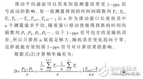
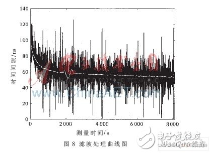
It can be seen from equation (4) that the calculation of frequency deviation only requires the measured value at the end of the window and is not affected by the measured value in the window. In actual application, the amount of calculation is small and simple, and it is convenient to use the PicoBlaze soft core processor to achieve. The FIFO data buffer connected to PicoBlaze is used to store the measurement data in the sliding window. When the storage reaches the preset window length, the previous measurement value will be read out from the FIFO sequentially, and the current measurement value will be matched to calculate the frequency deviation according to formula (3). The white curve in Fig. 8 is the time interval of the system output after filtering is added. The comparison shows that the filtering has a good suppression effect on jitter and large jump points.
The crystal oscillator frequency calibration system introduced in this article uses the standard second pulse signal output by the GPS module to calibrate the local crystal oscillator frequency. This design implements a high-resolution time interval measurement unit based on the carry logic resources inside the FPGA, and uses the PicoBlaze processor to process the measured time interval data in real time with the moving average filtering method. It can not only accurately measure the time interval between the local crystal oscillator frequency division signal and the GPS second pulse signal, but also reduces the interference of GPS second pulse fluctuations on the measurement results, and provides reliable correction data for the calibration of the crystal oscillator frequency. In addition, the measurement and control part of the system is completely implemented in FPGA, which helps to improve the measurement resolution, reduce the system volume, and improve the stability of system operation. This system can be used not only in magnetotelluric three-dimensional acquisition stations, but also in other instruments that require frequency accuracy.
R&M Vape,R&M Disposable Vape,R&M Legend Pro Disposable Vape,R&M Vape Pen
Shenzhen Uscool Technology Co., Ltd , https://www.uscoolvape.com