In the field of switching power supplies from line voltage AC to low voltage DC, flyback is the most popular topology. One of the main reasons for this is its unique cost-effectiveness, which requires only adding additional windings to the transformer secondary to provide multiple output voltages.
Typically, the feedback comes from the output that has the most stringent requirements for output tolerance. This output then defines the number of volts per volt of all other secondary windings. Due to the leakage inductance effect, the output terminal cannot always achieve the desired output voltage cross-regulation, especially if the output is overloaded or the load is extremely light due to the full output of the other output.
A post-stage regulator or dummy load can be used to prevent the output voltage from rising in such cases. However, because post-stage voltage regulators or dummy loads can cause cost increases and reduced efficiency, they lack sufficient attractiveness, especially in recent years for no-load and/or standby input power consumption in a variety of consumer applications. This design began to be left out when regulations were becoming more stringent. The active shunt regulator shown in the figure not only solves the regulation problem, but also minimizes the cost and efficiency impact.

The circuit works as follows: When both outputs are in regulation, the resistor dividers R14 and R13 bias the transistor Q5, which keeps Q4 and Q1 off. Under such operating conditions, the current flowing through Q5 acts as a small dummy load on the 5V output.
The standard difference between the 5V output and the 3.3V output is 1.7V. When the load requires additional current from the 3.3V output, and the load current output from the 5V output does not increase by the same amount, its output voltage will rise compared to the 3.3V output voltage. Since the voltage difference is approximately over 100 mV, Q5 will be biased off, turning on Q4 and Q1 and allowing current to flow from the 5V output to the 3.3V output. This current will reduce the voltage at the 5V output, which in turn will reduce the voltage difference between the two outputs.
The amount of current in Q1 is determined by the voltage difference between the two outputs. Therefore, the circuit keeps both outputs regulated without being affected by their load, even with the worst case where the 3.3V output is fully loaded and the 5V output is unloaded. The Q5 and Q4 in the design provide temperature compensation because the VBE temperature variations in each triode can cancel each other out. Diodes D8 and D9 are not required, but can be used to reduce power dissipation in Q1, eliminating the need to add heat sinks in the design.
This circuit reacts only to the relative difference between the two voltages and is essentially ineffective under full load and light load conditions. Since the shunt regulator is connected from the 5V output to the 3.3V output, the active dissipation of the circuit can be reduced by 66% compared to a grounded shunt regulator.
More about IN4005 information: IC query network http://
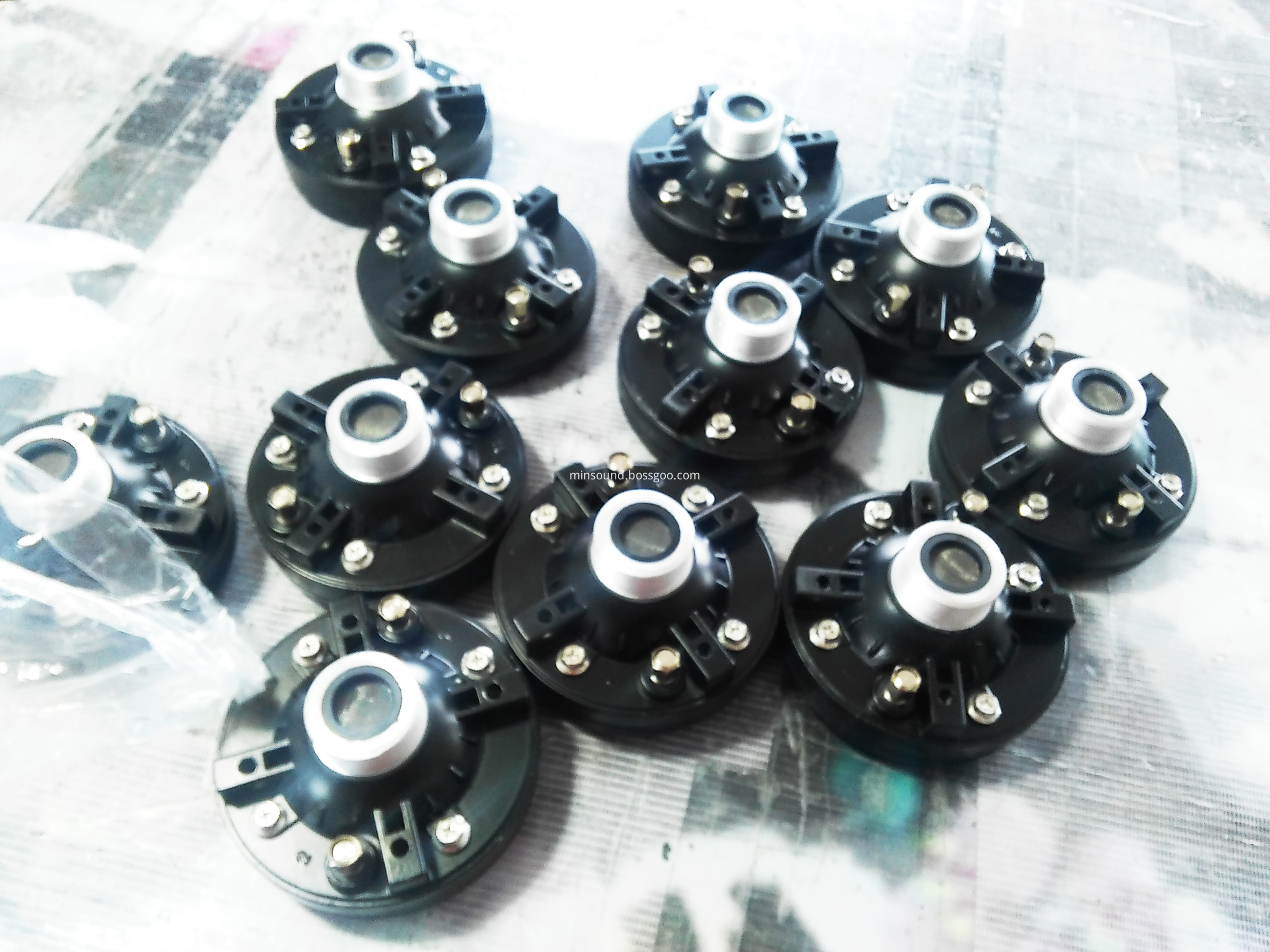
Minsound offers a great range of Driver Units,providing accurate reproduction.high intelligibility and dependable performance in commercial sound,signaling and public address loudspeaker systems.
All models are suited for Minsound reflex horns,equipped with the industry standard 1-3/8"-male tread pattern.
This series driver units are made of Neodymium magnet for good performance.
Neodymium Driver Units,Neodymium Driver,Neodymium Drivers,neodymium speaker magnets,Neodymium magnets
Taixing Minsheng Electronic Co.,Ltd. , https://www.ms-speakers.com