The basic working principle of the thyristor is embodied in the resistance state, the on state, and the conversion between the resistance state and the on state.
First look at the reverse blocking state of the thyristor. When the gate of the thyristor is open and the anode and cathode are in reverse bias, that is, when the anode potential is low and the cathode potential is high, the space charge area distribution and electron and hole flow in the thyristor are shown in Figure 1. At this time, the J2 junction is positively biased, and the J1 and J3 junctions are reverse biased. Assume that the injection efficiency of the J2 junction is 1 in the figure. Due to the high impurity concentration on both sides of the J3 junction (heavy doped regions), Zener breakdown occurs under low voltage, and there is no ability to withstand voltage, and the voltage is almost all applied to the J1 junction. Therefore, the reverse characteristic of the device is similar to that of a single PN junction device. When the applied voltage increases to the avalanche breakdown voltage of the J1 junction, a reverse breakdown phenomenon occurs.
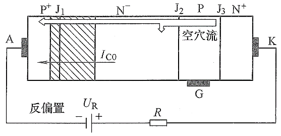
Figure 1 Schematic diagram of carrier flow when the thyristor is blocked by reverse bias
Then look at the positive blocking state of the thyristor. When the gate of the thyristor is open and the anode and cathode are in a forward bias, that is, when the anode potential is high and the cathode potential is low, the space charge area distribution and electron and hole flow in the thyristor are shown in Figure 2.
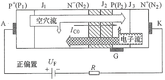
Figure 2 Schematic diagram of carrier flow when the thyristor is blocked
At this time, the J2 junction is reverse biased, and the J1 and J3 junctions are forward biased, and the applied voltage almost all falls on the J2 junction. The current through the device is approximately the reverse saturation current of the J2 junction, and the device is in a forward blocking state. The holes and electrons injected through the positive bias minority carrier injection effect of the J1 and J3 junctions are partially recombined in the N1 and P2 regions respectively, and then are extracted to the P2 and N1 regions through the reverse bias minority carrier extraction effect of the J2 junction. . When the applied voltage increases to the avalanche breakdown voltage of the J2 junction, the width of the space charge region of the J2 junction increases, the electric field increases, and a significant avalanche multiplication effect occurs. As a result, the current through the J2 junction increases, that is, the current through the device increases, and the original J2 junction reverse leakage current is transformed into a current multiplied by the J2 junction avalanche, and the device is in a turning state. The N1 and P2 areas on both sides of the J2 junction begin to accumulate electrons and holes before they can recombine. On the one hand, these accumulated carriers compensate the impurity ions in the space charge region of the J2 junction, narrow the width of the space charge region, weaken the electric field, and weaken the avalanche multiplier effect, which can offset the applied voltage and cause the withstand voltage to decrease; on the other hand, , The holes accumulated in the P2 area and the electrons accumulated in the N1 area increase the potential of the P2 area and decrease the potential of the N1 area, which causes the positive bias voltage of the J3 and J1 junctions to increase, the forward injection effect increases, and the current through the J2 junction further increases . With the continuous accumulation of carriers on both sides of the J2 junction, the electric field in the space charge region and the avalanche multiplication effect are also constantly weakened. When the avalanche multiplication effect is completely eliminated, the charge accumulation on both sides of the J2 junction can still be maintained. In this way, J1, J3 The positive injection of the junction reaches the carriers accumulated on both sides of the J2 junction, and finally the J2 is changed from a negative bias to a positive bias. The three junctions are all in forward bias, allowing a large current to pass, and the device is in a forward conducting state. The overall effect is that even in the case of an open gate, the forward voltage of the thyristor gradually increases to a turning voltage and then begins to enter the conduction state. When the gate has current input, the turning voltage will decrease.
For the reverse blocking state, there will be no accumulation of carriers on both sides of the pressure bearing, so there is no transition voltage into the conduction state.
Finally, look at the conduction state of the thyristor. When the thyristor is in the on state, a large number of unbalanced carriers accumulate on both sides of the J2 junction. When the current flowing through the thyristor is large, the concentration of excess carriers accumulated by the injection into the N1 and P2 regions is too late to recombine and is much greater than the concentration of impurity atoms in these two regions, so that both regions behave like The intrinsic region is the same. At this time, the entire thyristor looks like a PIN diode (the thyristor is in the hold and does not require gate current to flow), and its on-state characteristics are the same as the PIN diode. But when the current flowing through the thyristor is small, the working principle of its on-state is more complicated. Studies have found that when the current flowing through the thyristor is small to a certain extent, only part of the device area in the large-area thyristor is open. There is a transition zone between the open part and the non-conductive part, as shown in Figure 3.
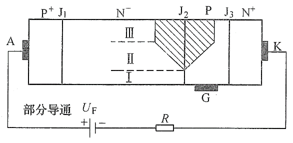
Figure 3 The conduction of the thyristor when a small current flows
Among them, zone I is the conducting zone, zone II is the transition zone, and zone III is the non-conducting zone. If the current flowing through increases slowly, the open area will gradually expand.
In order to quantitatively analyze the turn-on and on-state conditions of the thyristor, a two-transistor equivalent circuit can be used. The process of disassembling the PNPN structure thyristor into two interconnected PNP and NPN transistors is shown in Figure 4. The collector of one transistor is also the substrate of the other transistor. This structure forms an internal positive feedback connection. . The interaction of the two PN junctions in each transistor is reflected in the current amplification factor of the transistor. The current amplification coefficients of the two transistors are α1 and α2 respectively. At this time, there is no need to consider the electron and hole current distribution inside the transistor. The current amplification coefficient is directly used to connect the collector and emitter currents of the transistor, and the thyristor can work. The principle is discussed.
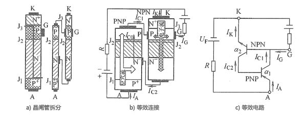
Figure 4 Two-transistor model of thyristor
When a forward voltage is applied to the thyristor, if the gate is also applied with a forward voltage, a current IG flows from the gate to the base of the NPN tube. After the NPN tube is turned on, its collector current IC2 flows into the base of the PNP tube and turns it on, so the collector current IC1 of the tube flows into the base of the NPN tube. Such a reciprocating cycle forms a strong positive feedback process, causing both transistors to be saturated and conducting, so that the thyristor quickly changes from the blocking state to the conducting state.
Note that IA and IK are the emitter currents of the PNP and NPN tubes respectively, then

Under the action of the internal electric field of the J2 junction, the reverse leakage current flowing through the junction is IC0, and the anode current of the thyristor is

Assuming that the gate current of the transistor is IG, the cathode current of the thyristor is

Combined, the anode current of the thyristor is

It can be seen that when the thyristor is in a forward bias, when the sum of the current amplification coefficients of the two transistors tends to 1, the anode current tends to infinity (or determined by the external circuit), and the thyristor is triggered by the gate signal Conduction. Therefore, the necessary conditions for the thyristor to trigger conduction are:

When the forward bias voltage is extremely high, the J2 junction will be multiplied by the carrier. If there is a multiplication factor M, the above relationship becomes

This is that when there is a gate current in the previous analysis, the transition voltage of this positive resistance state will decrease.
In the analysis of the transistor, it is known that the current amplification factor of the transistor is not a constant, but changes with the current flowing through it. The same is true for the two equivalent transistor current amplification factors in the thyristor. The two current amplification factors of a certain thyristor are shown in Figure 5. When the thyristor can be turned on and the current flowing through it reaches a certain level, even if the gate current is not needed, the anode current can still be maintained. This phenomenon is called the holding effect. This is a very important difference between a thyristor and a transistor. The transistor turns off when there is no base current. Of course, there are many reasons for the change of the current amplification factor of each equivalent transistor, such as the displacement current caused by temperature, light or du/dt, which can all become the trigger conditions for the thyristor to enter the on-state from the resistance state.
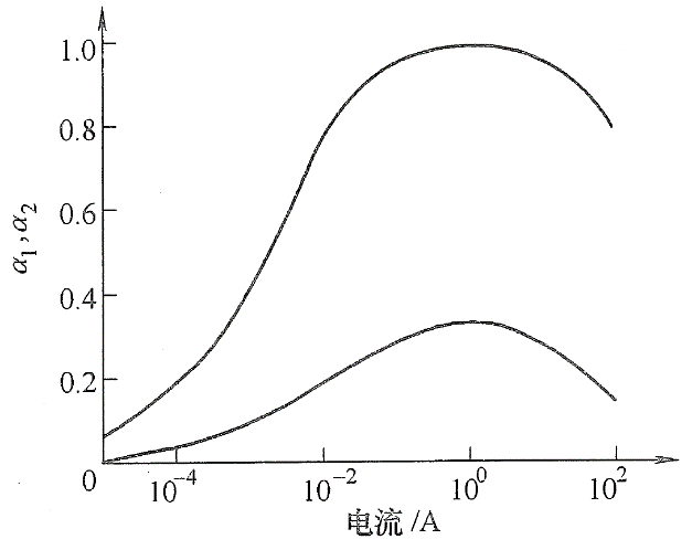
Fig. 5 The curve of current amplification factor changing with current
In summary, the volt-ampere characteristic curve of the thyristor is shown in Figure 6. Under the forward bias, the device is in the forward blocking state. When the bias voltage is high, the turning point occurs. The resistance state enters the on state. This state transition can be caused by voltage or gate current. Cause (or other reasons), when the gate is supplied with proper current, the thyristor can be turned on under a certain bias voltage. At this time, even if the gate current is removed, the device can still maintain the conduction state. It can be seen that once the thyristor is turned on, the gate will lose control. Therefore, the trigger current often uses pulse current instead of direct current. After being turned on, as long as the current flowing through the device gradually decreases to a certain value, the device can be restored to the blocking state. This kind of shut-off method is called natural shut-off. In addition, it can also be forced shut-off by applying a reverse bias voltage between the anode and the cathode. Under reverse bias, its volt-ampere characteristics are exactly the same as those of a diode.
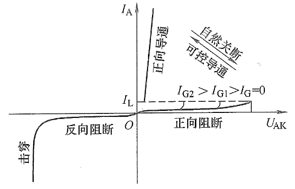
Figure 6 Schematic diagram of volt-ampere characteristics of thyristor
With the development of the times, the consumption level of people is gradually increasing. At the same time, people's entertainment methods are beginning to diversify, especially for modern young people. As a result, different kinds of electronic products are starting to be in people's lives, and the booming Electronic Cigarette industry reflects this.
Described including the upper shell, the upper shell at the top of the smoke outlet, as described in the bottom of the upper shell with airway, described with the smoke outlet in the airway and also to match the upper shell, the lower part of the shell described the airway in the direction of the lower shell extension, as described in the lower shell near one end of the upper shell is equipped with oil mouth, described the lower shell with batteries, described at the bottom of the bottom shell has come in The air port is provided with an oil storage bin in the lower shell, and the air passage passes through the oil storage bin and is provided with a heating atomization bin at one end away from the smoke outlet. The utility model has beneficial effects: it can meet the smoking habit of different users, avoid the premature end of the use experience caused by excessive consumption of smoke oil, and indirectly prolong the service time and life of the product.
Refillable E-Cig Oem,Refillable Vape Pod,Refillable Vape Pen Oem,Refillable Mod Oem
Shenzhen MASON VAP Technology Co., Ltd. , https://www.e-cigarettefactory.com