Precision analog designers often rely on quiet, low-noise reference sources to power DACs and ADC converters. This task is not within the basic responsibility of the reference, and it is designed on the surface to provide a clean and accurate stable voltage for the actual power supply, ie the reference input of the power converter. With some considerations in mind, the voltage reference is usually able to perform the task of providing precise voltage to the converter's reference input. This allows the designer to boldly require the reference to supply power to higher and higher current applications. So, if the reference can power the converter, why not supply power to the analog signal chain, other converters, or other circuits?
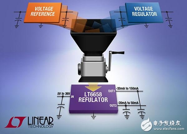
Any design flow usually involves the choice of accuracy and power consumption. To make a choice, a rough approach suggests using a voltage reference when accuracy is required and using an LDO when milliwatt power consumption is required. In addition to the additional board space and cost, it is also necessary to route different signals regardless of whether the nominal voltage is the same or not. If a high-precision voltage source is needed to provide milliwatt-level power, designers will have to buffer the reference. The LT6658 solves this problem by providing two low-noise, high-precision outputs with a combined output current of 200 mA and a world-class reference voltage specification.
About LT6658 - Low Drift Regulator for Reference Quality
The LT6658 is a precision low-noise, low-drift regulator with the accuracy specifications of a dedicated reference and the power capabilities of a linear regulator - combining the advantages of both with ADI's RefulatorTM technology. The LT6658 has a drift of 10 ppm/°C and an initial accuracy of 0.05%. Both outputs support 150 mA and 50 mA, respectively. Each output has an active 20 mA active current sink capability. To maintain high accuracy, the load regulation is 0.1 ppm/mA. When the input voltage source pins are connected together, the voltage regulation rate is typically 1.4 ppm/V, and when an independent supply is provided to the input pins, the voltage regulation rate is less than 0.1 ppm/V.
To better understand the features of the LT6658 and how it achieves this high level of performance, Figure 1 shows a typical application. The LT6658 consists of a reference voltage level, a noise reduction stage, and two output buffers. The reference voltage is supplied separately from the two output buffers for excellent isolation. Each output buffer has a Kelvin sense feedback pin to provide optimum load regulation.
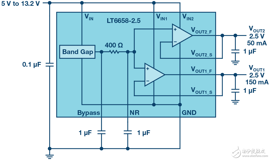
Figure 1. Typical application
The noise reduction stage consists of a 400 Ω resistor and a pin for connecting an external capacitor. The RC network acts as a low-pass filter to limit the noise bandwidth of the reference voltage level. The external capacitor can be arbitrarily large to reduce the noise bandwidth to very low frequencies.
Fast and Quiet Load Step Response As a regulator, the LT6658 supplies 150 mA from the VOUT1_F pin and has excellent transient response performance. Figure 2a shows the device's response to a 1 mA load step transient (from 10 mA to 11 mA); Figure 2b shows the device's response to a 140 mA load step transient (from 10 mA to 150 mA). The output current and current sink capability of the output buffer allow the output to be quickly established. The transient response time is very short while maintaining excellent load regulation. The load regulation is typically 0.1 ppm/mA. The second output VOUT2_F has similar response performance with a maximum load of 50 mA.
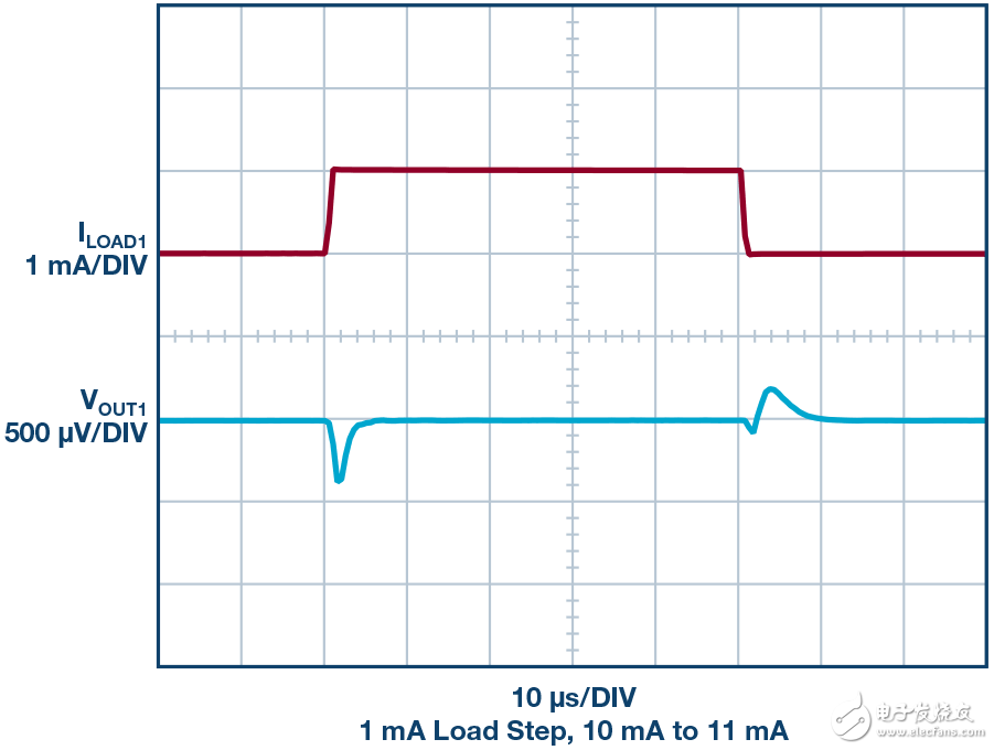
Figure 2a. 1 mA Load Step Response
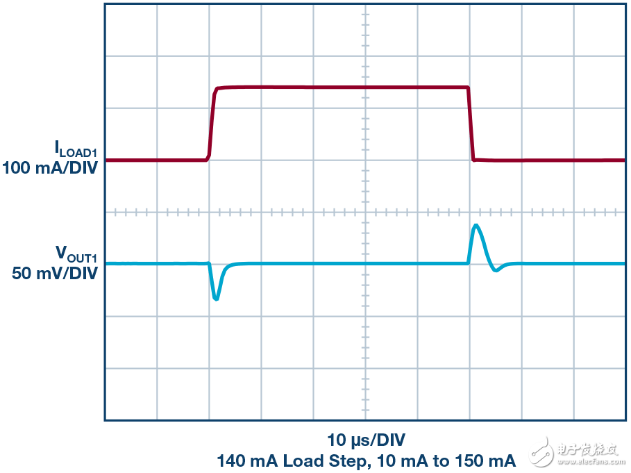
Figure 2b. 140 mA Load Step Response
Output Tracking For multiple converter applications with different reference voltages, even if the output is set to a different voltage, the output of the LT6658 is tracked to ensure that the conversion results are consistent. This is possible because the LT6658's two outputs are driven by a common voltage source. The output buffer is adjusted for excellent tracking and low drift. When the load on VOUT1_F increases from 0 mA to 150 mA, the VOUT2 output changes by less than 12 ppm, as shown in Figure 3. In other words, even if the load and working conditions change, the relationship between the output can be well maintained.
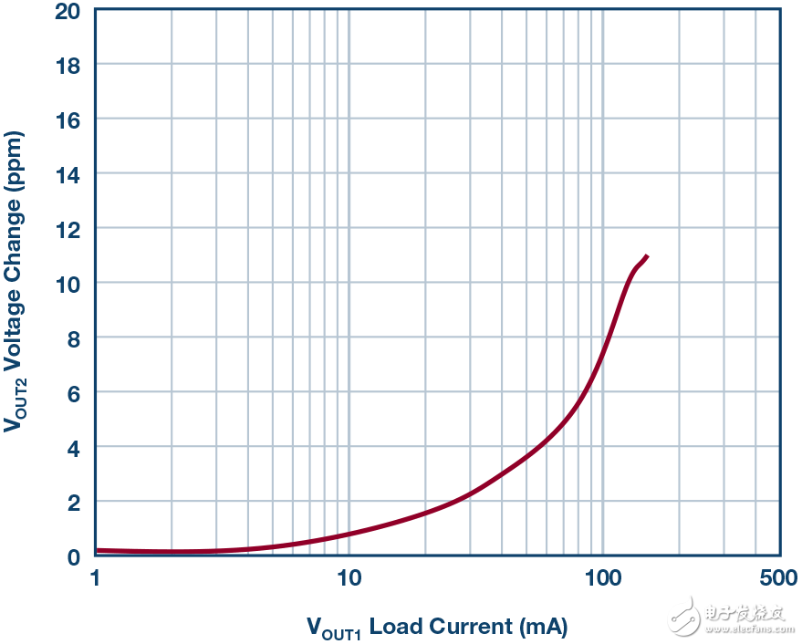
Figure 3. Load Adjustments Between Channels (Eliminates Fever Effects)
Power Suppression and Isolation To help achieve excellent power supply rejection and output isolation, the LT6658 offers three power supply pins. The VIN pin powers the reference circuit, and VIN1 and VIN2 power VOUT1 and VOUT2, respectively. The simplest method is to connect all three power pins together to provide a typical DC power supply rejection of 1.4 ppm/V. When the power pins are connected separately and VIN1 power is switched, the VOUT2 dc voltage regulation is 0.06 ppm/V.
Table 1 summarizes the power supply rejection when each supply pin changes from 5 V to 36 V. The VIN supply has the highest sensitivity, resulting in a typical output change of 1.4 ppm/V. The power pins VIN1 and VIN2 have almost no effect. The measurement result in the VIN1 and VIN2 columns is the output noise level.
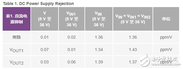
Table 4 shows two examples of AC PSRR. The first example has a 1 μF capacitor on the NR pin. The second example has a 10 μF capacitor on the NR pin. The larger 10 μF capacitor extends the 107 dB rejection to 2 kHz.
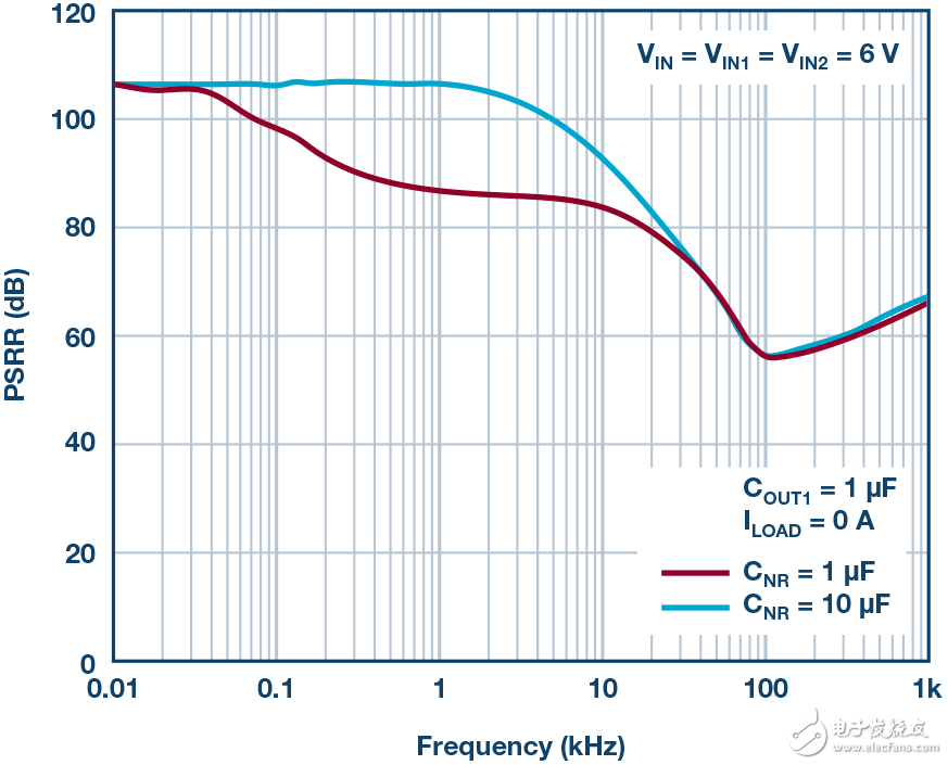
Figure 4. Power supply ripple rejection
Figure 5 shows the AC channel isolation from VIN1 to VOUT2. When CNR = 10 μF, the power isolation between channels above 100 kHz is greater than 70 dB.
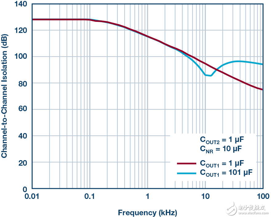
Figure 5. VOUT1 to VOUT2 isolation between channels
Load transients have minimal effect on adjacent outputs. Figure 6a and Figure 6b show the output isolation between channels. While one output is swinging at 50 mV rms, plot the other output change.
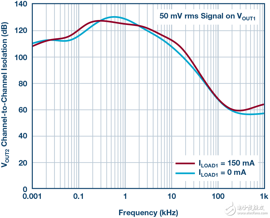
Figure 6a. VOUT1 to VOUT2 Load Regulation Between Channels
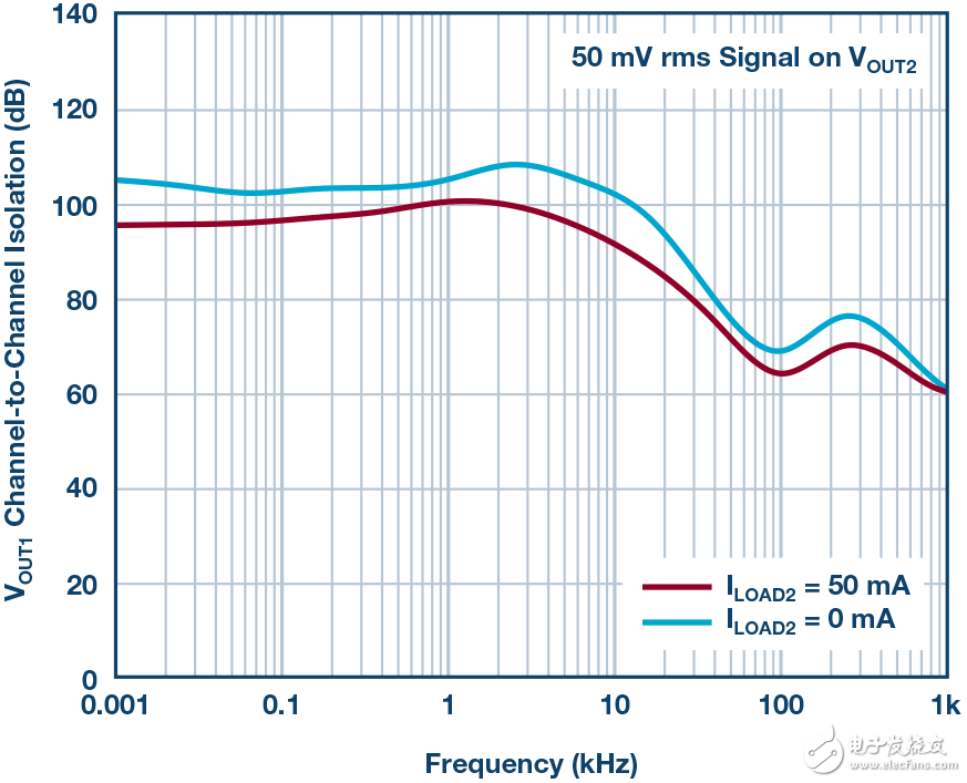
Figure 6b. VOUT2 to VOUT1 Load Regulation Between Channels
Using the circuit shown in Figure 7 can achieve extraordinary AC PSRR. VOUT1 outputs the power supplies VIN and VIN2 to generate a recursive reference.
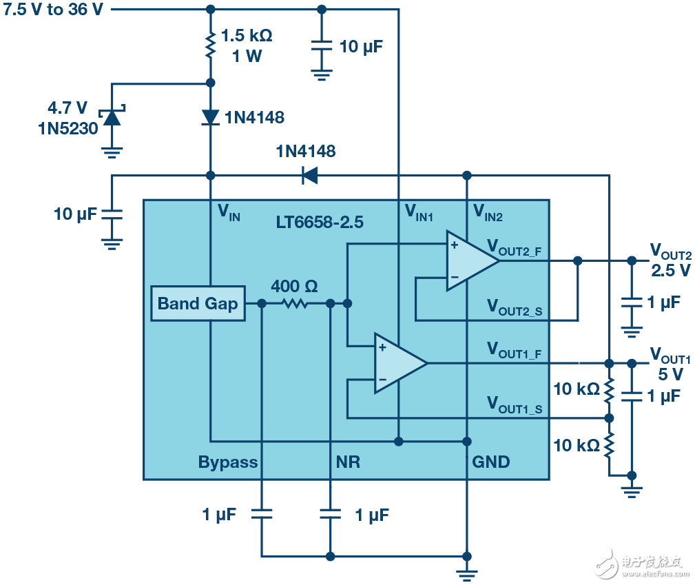
Figure 7a. Recursive Voltage Reference Solution (VOUT1 powered by VIN and VIN2)
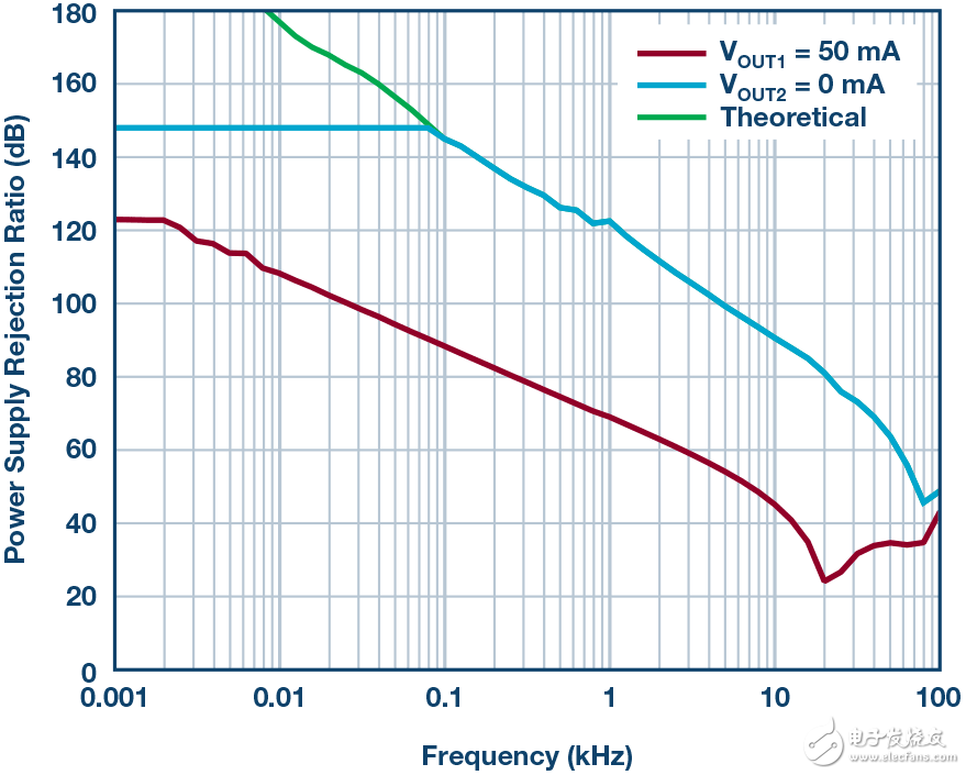
Figure 7b. AC PSSR for recursive reference circuit
Power Management and Protection The three power pins help manage the power consumption of the package. When providing large currents, the supply voltage should be reduced to minimize the power consumption of the LT6658. The voltage appearing on the output device will be small, reducing power consumption and increasing efficiency.
The output disable pin OD is used to turn off the output buffer and place the VOUT_F pin in a high-impedance state. This is useful in the event of a failure. For example, the load may be damaged and short-circuited. This event can be detected by an external circuit and both outputs can be disabled. This feature can be ignored. When the OD pin is left floating or connected high, a weak pull-up current will enable the output buffer.
The LT6658 is available in a 16-lead MSE exposed pad package with θJA as low as 35°C/W. When the supply voltage is high, the power efficiency is low, resulting in overheating of the package. For example, a 32.5 V supply voltage at full load will generate 30 V &TImes; 0.2 A of excess power on the output device. The extra power of 6 W will increase the internal temperature of the chip to 210°C above the ambient temperature, which is very dangerous. To protect the device, the thermal shutdown circuit disables the output buffer when the die temperature exceeds 165°C.
Noise Noise is an important consideration for data converters and other precision applications. Adding a capacitor to the NR (noise reduction) pin can further reduce the noise of the low noise LT6658. The capacitor on the NR pin forms a low-pass filter with the on-chip 400 Ω resistor. Large capacitors will reduce the filter frequency, thereby reducing the total integrated noise. Figure 8 shows the effect of increasing the capacitance on the NR pin. With a 10 μF capacitor, the noise roll drops to about 7 nV/√Hz.
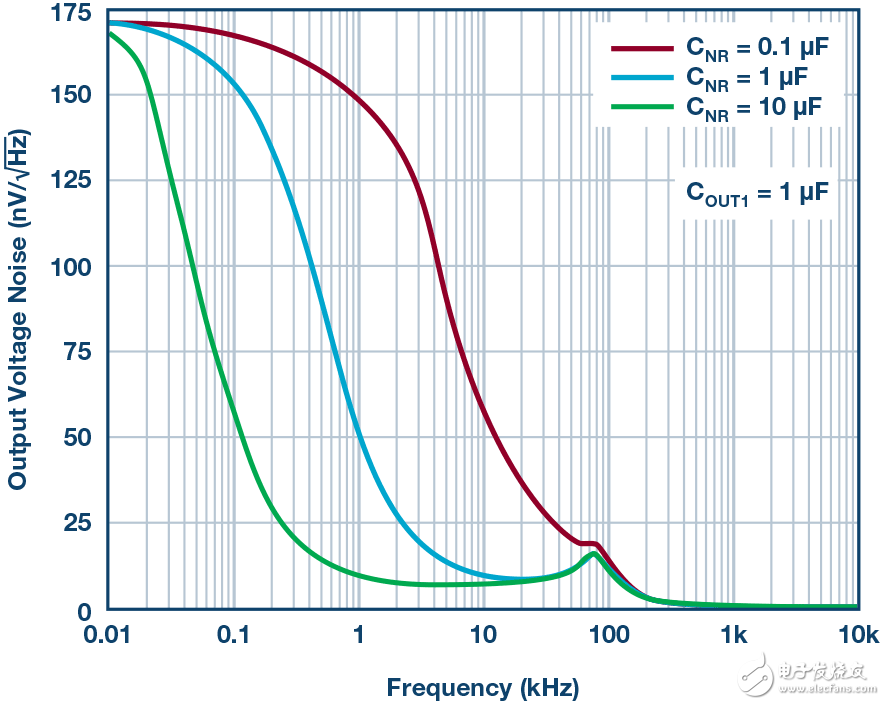
Figure 8. Reduce noise by increasing CNR
By increasing the output capacitance, noise can be further reduced. When both NR and output capacitance increase, the output noise can fall to a few microvolts. The LT6658 is stable when the output capacitance is between 1 μF and 50 μF. If a 1 μF ceramic capacitor is connected in parallel, the output remains stable under large capacitance. For example, in the circuit shown in Figure 9a, a 1 μF ceramic capacitor is connected in parallel with a 100 μF polymer aluminum capacitor. This configuration can maintain stability while reducing the noise bandwidth. Figure 9b shows the noise response for different output capacitor values. In all three cases, there is a small 1 μF ceramic capacitor in parallel with the larger capacitor.
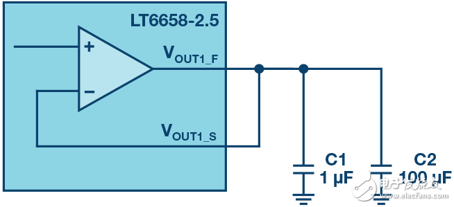
Figure 9a. Reduce noise by increasing C1
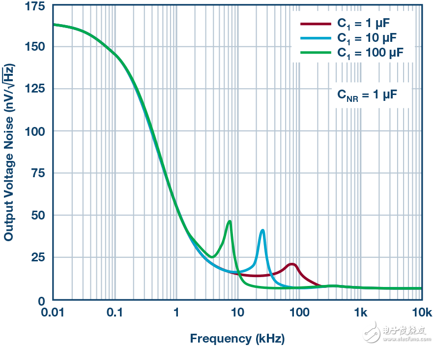
Figure 9b. Noise reduction by increasing C1
One drawback of this scheme is the noise peaking, which may increase the total integrated noise. To reduce noise peaking, a 1 Ω resistor can be inserted in series with the large output capacitor, as shown in Figure 10a. The output voltage noise and total integrated noise are shown in Figures 10b and 10c, respectively.
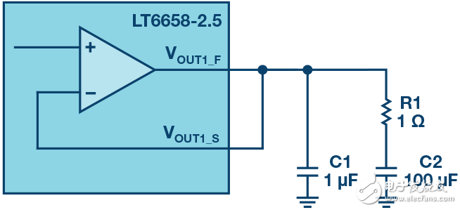
Figure 10a. Reduce noise peaking by adding a 1 Ω resistor in series with C2
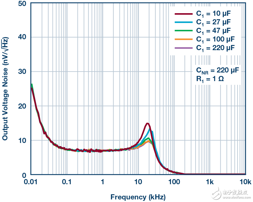
Figure 10b. Reduce noise peaking by adding a 1 Ω resistor in series with C2
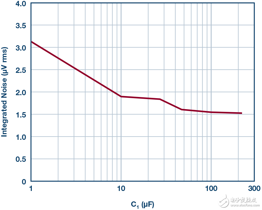
Figure 10c. Reduce noise peaking by adding a 1 Ω resistor in series with C2
application
The LT6658 provides a quiet and precise power supply for many demanding applications. In the mixed-signal field, data converters are often controlled by microcontrollers or FPGAs. Figure 11 shows the basic principle. The sensors provide signals to analog processing circuits and converters, all of which require a clean power supply. The microcontroller may have multiple power inputs, including analog power.
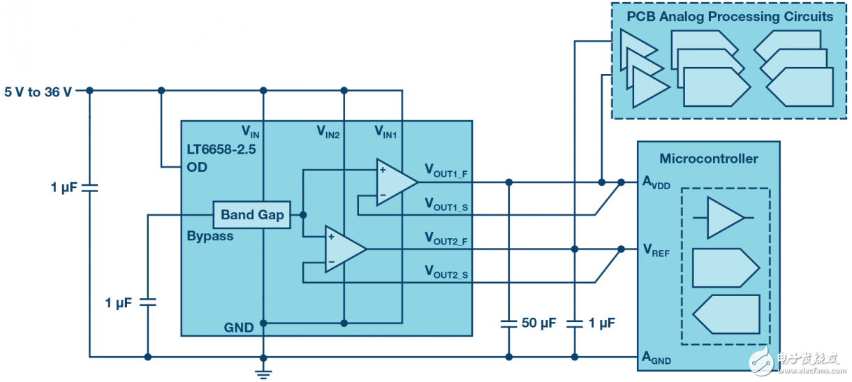
Figure 11. Mixed Signal Application
As a general rule, the microcontroller's high-noise digital supply voltage should be isolated from clean precision analog supplies and reference sources. The LT6658's two outputs provide excellent channel-to-channel isolation, power supply rejection, and supply current capability, ensuring clean power for multiple sensitive analog circuits.
The LT6658 is also well-suited for industrial environments because it can operate with a noisy supply rail and load glitches caused by conversions at one output have little effect on adjacent outputs. In addition, when the load on one output needs current, the adjacent output will continue to track.
Figure 12 shows a practical example where the LTC2379-18 high-speed ADC circuit is powered by the LT6658. The Kelvin detection input on VOUT2 is configured to boost the 2.5 V output to the 4.096 V reference and provide the common-mode voltage to the input amplifier LTC6362. VOUT1 rises to 5 V and powers the LTC6362 and other analog circuits that require a 5 V supply. The LT6658's two outputs have 150 mA and 50 mA maximum load on VOUT1 and VOUT2, respectively.
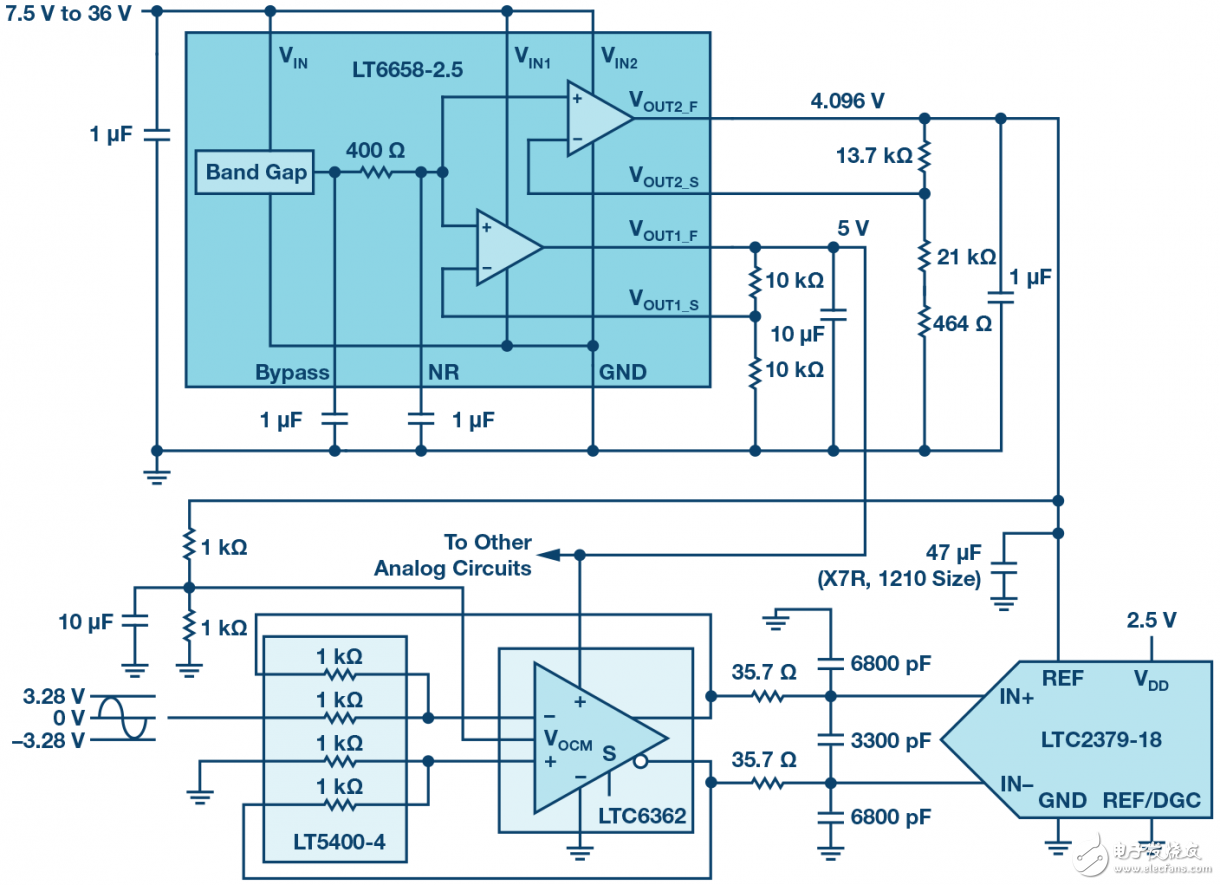
Figure 12. Data Acquisition Solution
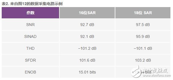
The circuit in Figure 13 shows how the LT6658 can power a noisy digital circuit while providing a quiet, accurate reference voltage for a precision ADC. In this application, one channel of the LT6658 or a separate LDO provides 3.3 V for the high-noise FPGA (VCCIO) and some other logic, while the other channel provides 5 V for the 20-bit ADC's reference input.
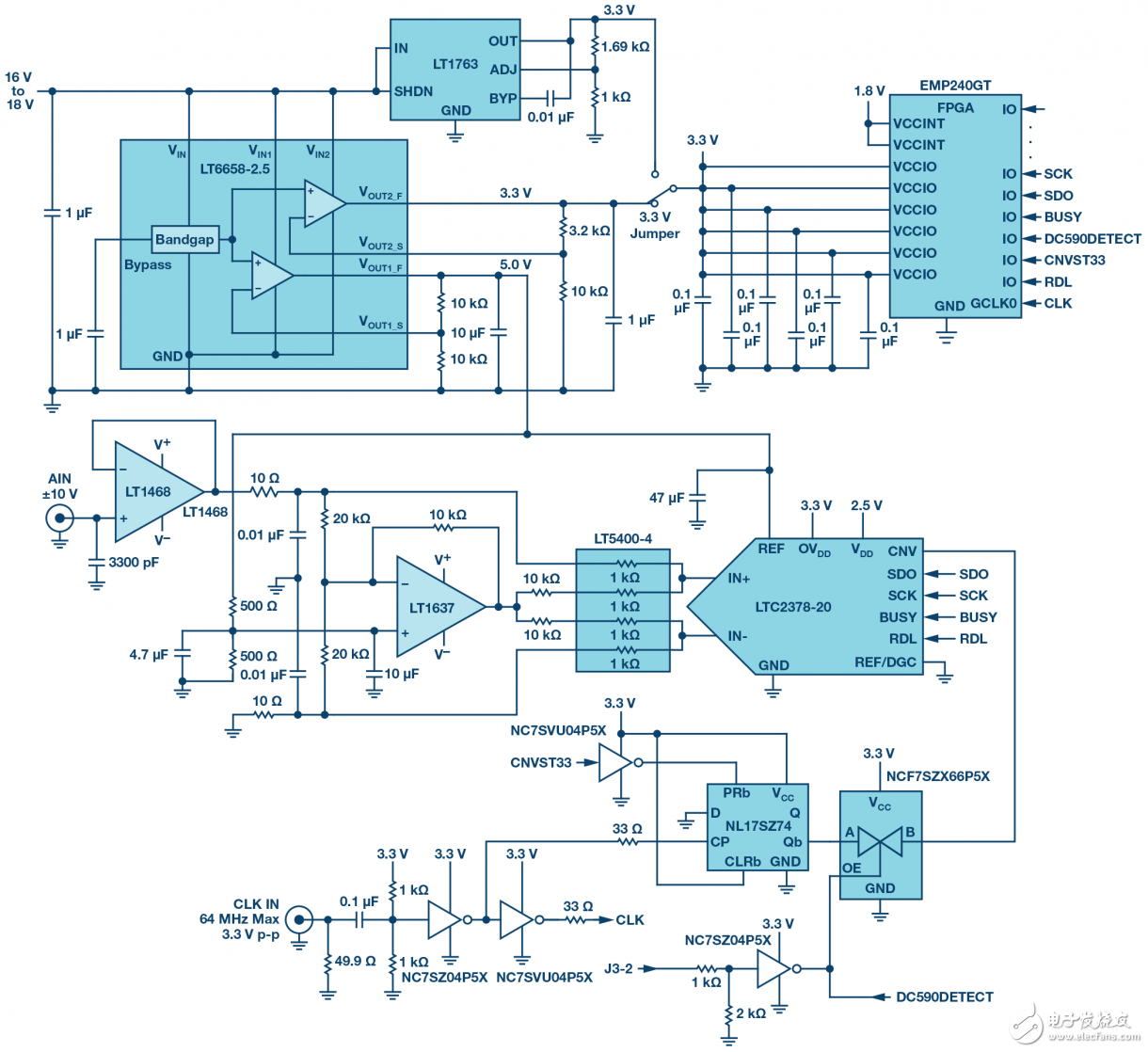
Figure 13. High-noise digital test example circuit
By switching the digital supply circuit between the LT6658 and the LDO, we can evaluate the ability of the LT6658 to isolate the digital noise on one channel from the other channel that drives the quiet reference input of the 20-bit ADC. Using a clean DC power supply at the ADC input, noise can be inferred, as shown in Figure 14. The histogram shows no significant difference in the results of the LT6658 or LDO powering the VCCIO pin of the FPGA, demonstrating the LT6658's robust regulation and isolation capabilities.
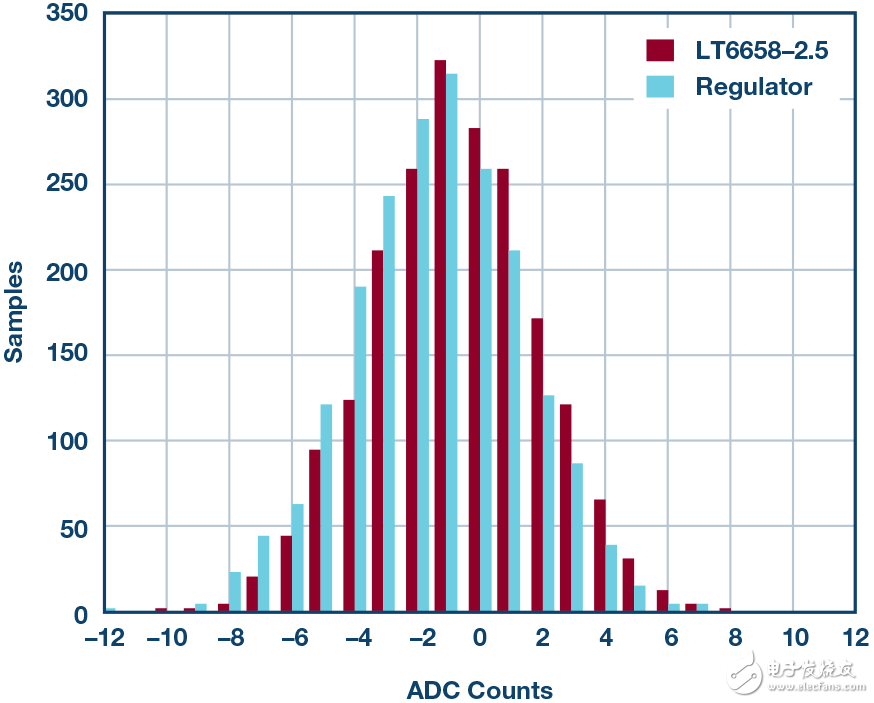
Figure 14. Test result histogram of the circuit shown in Figure 13.
Conclusion
The LT6658 is the next step in the development of reference and regulators. For precision analog power supplies, the precise performance and capability to deliver 200 mA combined current from a single package is a paradigm shift. Noise suppression, channel-to-channel isolation, tracking and load regulation make this product ideal for precision analog voltage references and power solutions. With this new method, the application does not require sacrificing accuracy or power consumption.
10-inch tablet devices have greatly surpassed netbooks in terms of entertainment, including reading, games, and audio-visual enjoyment. In other respects, the basic operation of the 10-inch tablet computer built on the touch screen ensures that the application of the tablet computer can be well realized, and its operation performance is closer to that of a smartphone.
1.In appearance, the 10-inches tablet computer looks like a large-screen mobile phone, or more like a separate LCD screen.
2.In terms of hardware configuration, the 10-inches tablet computer has all the hardware devices of a traditional computer, and has its own unique operating system, compatible with a variety of applications, and has a complete set of computer functions.
3.The 10-inches tablet computer is a miniaturized computer. Compared with traditional desktop computers, tablet computers are mobile and flexible. Compared with Laptops, tablets are smaller and more portable
4.The 10-inches tablet is a digital notebook with digital ink function. In daily use, you can use the tablet computer like an ordinary notebook, take notes anytime and anywhere, and leave your own notes in electronic texts and documents.
10 Inches Tablet Pc,Tablet Pc Android,10 Inch Quad Core Tablet,Tablet 10 Inch
Jingjiang Gisen Technology Co.,Ltd , https://www.jsgisentec.com